GENERAL DESCRIPTION
The AD9854 digital synthesizer is a highly integrated device that uses advanced DDS technology, coupled with two internal high speed, high performance quadrature DACs to form a digitally programmable I and Q synthesizer function. When referenced to an accurate clock source, the AD9854 generates highly stable, frequency-phase, amplitude-programmable sine and cosine outputs that can be used as an agile LO in communications, radar, and many other applications. The innovative high speed DDS core of the AD9854 provides 48-bit frequency resolution (1 μHz tuning resolution with 300 MHz SYSCLK). Retaining 16 bits for phaseto-amplitude conversion ensures excellent spurious-free dynamic range (SFDR). The circuit architecture of the AD9854 allows the generation of simultaneous quadrature output signals at frequencies up to 150 MHz, which can be digitally tuned at a rate of up to 100 million new frequencies per second. The sine wave output (externally filtered) can be converted to a square wave by the internal comparator for agile clock generator applications. The device provides two 14-bit phase registers and a single pin for BPSK operation. For higher-order PSK operation, the I/O interface can be used for phase changes. The 12-bit I and Q DACs, coupled with the innovative DDS architecture, provide excellent wideband and Data Sheet narrow-band output SFDR. The Q DAC can also be configured as a user-programmable control DAC if the quadrature function is not desired. When configured with the comparator, the 12-bit control DAC facilitates static duty cycle control in high speed clock generator applications. Two 12-bit digital multipliers permit programmable amplitude modulation, on/off output shaped keying, and precise amplitude control of the quadrature output. Chirp functionality is also included to facilitate wide bandwidth frequency sweeping applications. The programmable 4× to 20× REFCLK multiplier circuit of the AD9854 internally generates the 300 MHz system clock from an external lower frequency reference clock. This saves the user the expense and difficulty of implementing a 300 MHz system clock source. Direct 300 MHz clocking is also accommodated with either singleended or differential inputs. Single-pin conventional FSK and the enhanced spectral qualities of ramped FSK are supported. The AD9854 uses advanced 0.35 µm CMOS technology to provide a high level of functionality on a single 3.3 V supply. The AD9854 is pin-for-pin compatible with the AD9852 singletone synthesizer. It is specified to operate over the extended industrial temperature range of −40°C to +85°C.
FEATURES
300 MHz internal clock rate
FSK, BPSK, PSK, chirp, AM operation
Dual integrated 12-bit digital-to-analog converters (DACs)
Ultrahigh speed comparator, 3 ps rms jitter
Excellent dynamic performance
80 dB SFDR at 100 MHz (±1 MHz) AOUT
4× to 20× programmable reference clock multiplier
Dual 48-bit programmable frequency registers
Dual 14-bit programmable phase offset registers
12-bit programmable amplitude modulation and
on/off output shaped keying function
Single-pin FSK and BPSK data interfaces
PSK capability via input/output interface
Linear or nonlinear FM chirp functions with single-pin
frequency hold function
Frequency-ramped FSK
<25 ps rms total jitter in clock generator mode
Automatic bidirectional frequency sweeping
Sin(x)/x correction
Simplified control interfaces
10 MHz serial 2- or 3-wire SPI compatible
100 MHz parallel 8-bit programming
3.3 V single supply
Multiple power-down functions
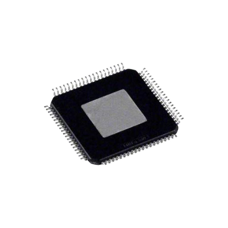
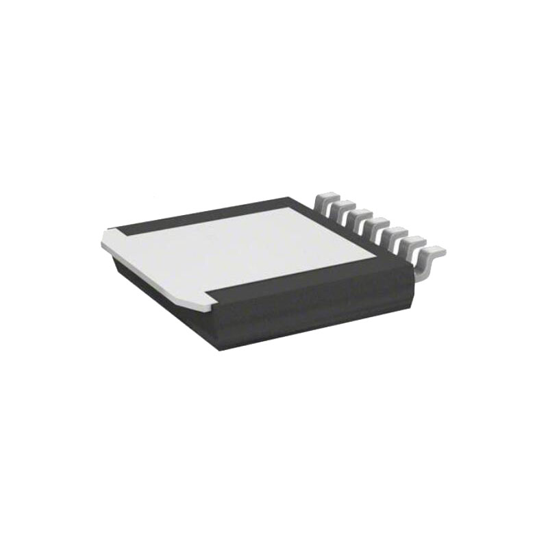
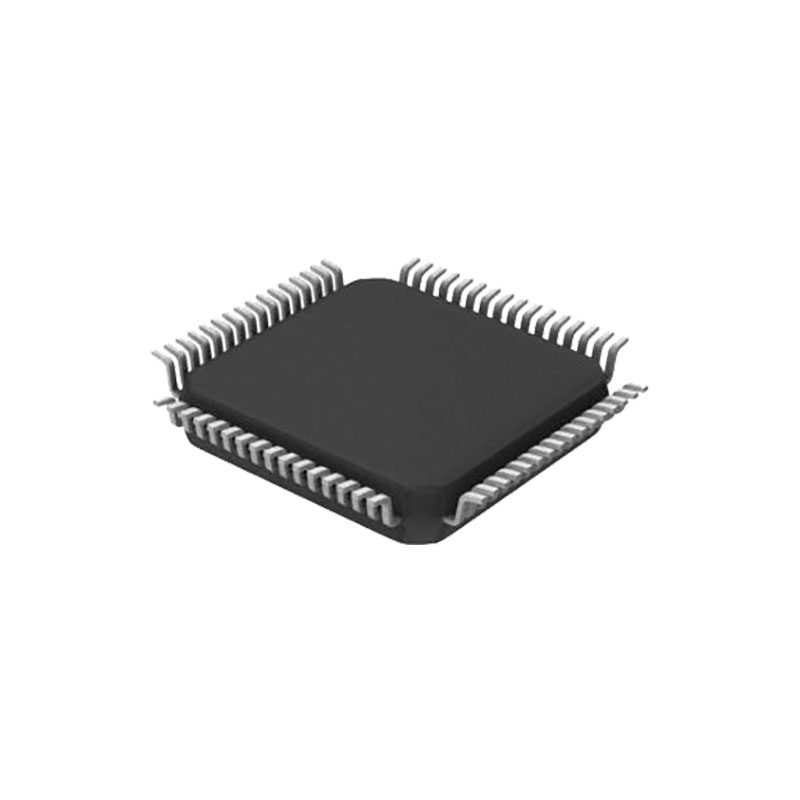
Single-ended or differential input reference clock Small, 80-lead LQFP or TQFP with exposed pad
APPLICATIONS
Agile, quadrature LO frequency synthesis
Programmable clock generators
FM chirp source for radar and scanning systems
Test and measurement equipment
Commercial and amateur RF exciters
THEORY OF OPERATION
The AD9854 quadrature output digital synthesizer is a highly flexible device that addresses a wide range of applications. The device consists of an NCO with a 48-bit phase accumulator, a programmable reference clock multiplier, inverse sinc filters, digital multipliers, two 12-bit/300 MHz DACs, a high speed analog comparator, and interface logic. This highly integrated device can be configured to serve as a synthesized LO, an agile clock generator, or an FSK/BPSK modulator. Analog Devices, Inc., provides a technical tutorial about the operational theory of the functional blocks of the device. The tutorial includes a technical description of the signal flow through a DDS device and provides basic applications information for a variety of digital synthesis implementations. The document, A Technical Tutorial on Digital Signal Synthesis, is available from the DDS Technical Library, on the Analog Devices DDS website at www.analog.com/dds.

