GENERAL DESCRIPTION
The ADF4368 is a high performance, ultra-low jitter, integer-N and fractional-N phase-locked loop (PLL) with integrated VCO ideally suited for frequency conversion applications.
The high performance PLL has a figure of merit of −239 dBc/Hz, very low 1/f noise of normalized −287 dBc/Hz and high PFD frequency that can achieve ultra-low in-band noise and integrated jitter. The ADF4368 can generate any frequency from 800 MHz to 12.8 GHz without an internal doubler, which eliminates the need for sub-harmonic filters. The Σ-Δ modulator includes a 25-bit fixed modulus that allows hertz frequency resolution and an additional 17-bit variable modulus, which allows even finer resolution and flexibility for frequency planning. The 9 dBm output power at 12.8 GHz in single-ended configuration with 16 step power adjust feature makes it very useful for any application.
For multiple frequency conversion applications, such as phase array radar or massive MIMO systems, the outputs of multiple ADF4368 can be aligned by using the SYNC input or EZSync™. The EZSync method is used when it is difficult to distribute the SYNC signal to all devices precisely. For applications that require deterministic delay or delay adjustment capability, a programmable reference to output delay with.
The simplicity of the ADF4368 block diagram eases development time with a simplified serial-peripheral interface (SPI) register map, external SYNC input, and repeatable multichip phase alignment both in integer mode and fractional mode.
FEATURES
► Output frequency range: 800 MHz to 12.8 GHz
► Jitter < 30 fsRMS fOUT = 9.001 GHz, fREF = fPFD = 250 MHz,fractional mode
► Wideband phase noise floor: −160 dBc/Hz at 12.8 GHz
► PLL specifications
► Normalized in-band phase noise floor
► −239 dBc/Hz: integer, −237 dBc/Hz: fractional mode
► Normalized 1/f phase noise floor
► −287 dBc/Hz: normalized to 1 Hz
► −147 dBc/Hz: normalized to 1 GHz at 10 kHz
► 625 MHz phase detector frequency integer mode
► 250 MHz phase detector frequency fractional mode
► 25-bit fixed, 49-bit combined fractional modulus
► 4 GHz reference input frequency
► Typical −95 dBc PFD spurs
► Reference to output delay specifications
► Temperature coefficient: 0.06 ps/°C
► Adjustment step size: <1 ps
► Multichip output phase alignment
► Through SYNC pin or by EZSync method
► 3.3 V and 5 V power supplies
► ADIsimPLL™ loop filter design tool support
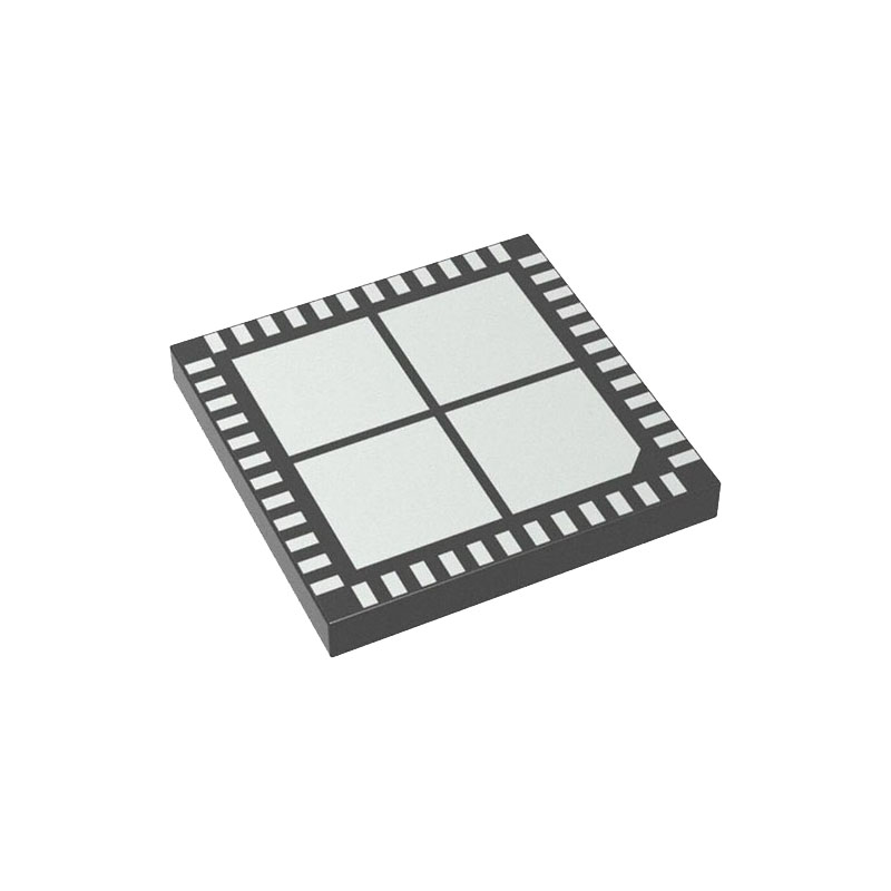
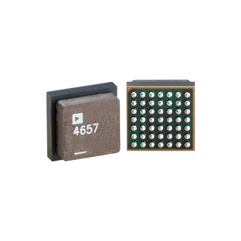
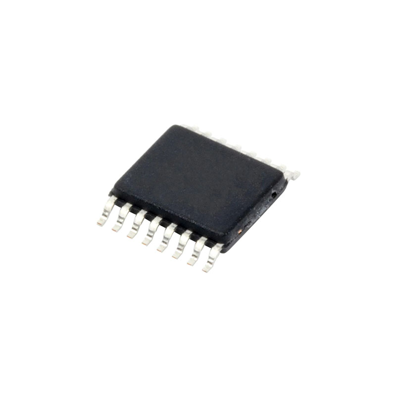
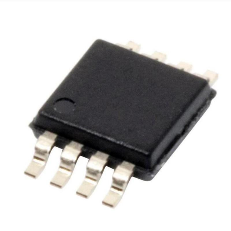
► Available in 48-lead, 7 mm × 7 mm LGA package
► −40°C to +125°C operating junction temperature
APPLICATIONS
► Wireless infrastructure (MC-GSM, 5G)
► Test and measurement
► Aerospace and defense
APPLICATIONS INFORMATION
POWER SUPPLY AND BYPASSING
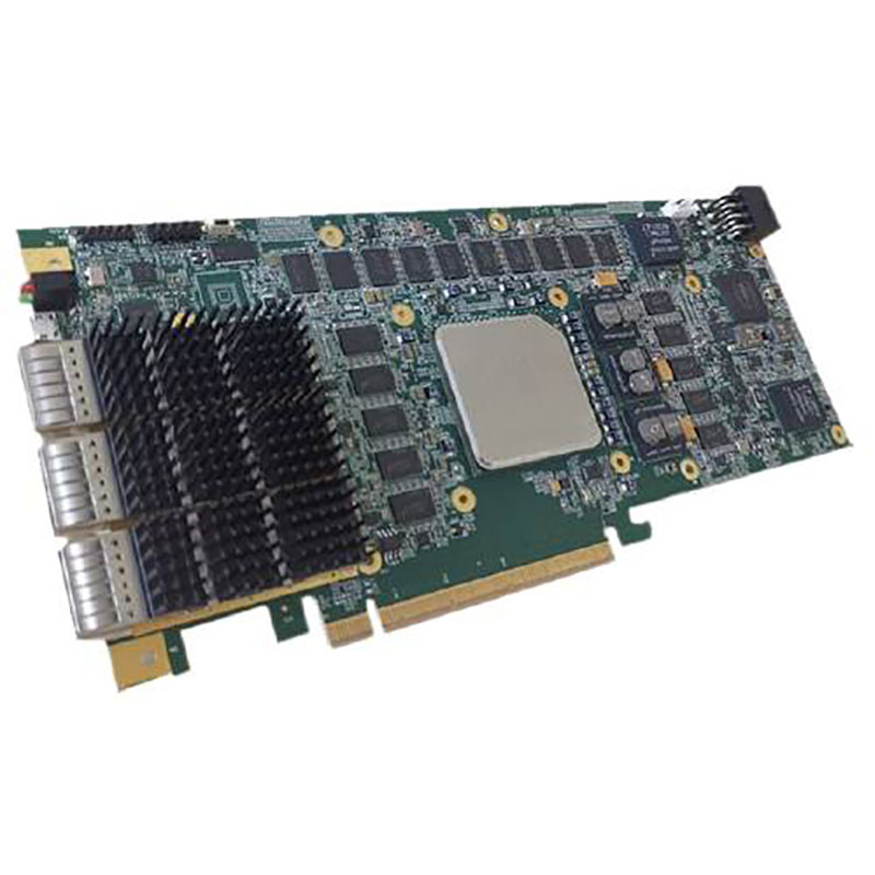
The ADF4368 is a high performance, low noise device. Phase noise and spurious performance may be degraded by noisy power supplies. To achieve maximum performance and ensure that power supply noise does not degrade the performance of the ADF4368, it is recommended to use the Analog Devices low noise, high pow er supply rejection ratio (PSRR) regulators. Preferred regulators include the LT3045, ADM7150, and the ADM7151. Additional exter nal supply bypass capacitors are also recommended. For more details, refer to the EVAL-ADF4368 evaluation board design.
LOOP FILTER DESIGN
A stable loop filter design requires care in selecting the loop filter components of the ADF4368. It is recommended to download and install ADIsimPLL™ for loop filter design and simulation. ADI simPLL™ has an integrated tutorial for first time users and a help manual for more complex topics. There are also several ADIsimPLL training videos available on www.analog.com. After a loop filter is designed and simulated, it is recommended to verify the new loop filter using the ADF4368 evaluation hardware.
A full loop filter design tutorial is beyond the scope of this data sheet. However, some best practices are shown in the following lists. ADIsimPLL aids in defining and simulating these parameters. Any significant change to these items requires a new loop filter design.

