General Description
The MAX629 low-power DC-DC converter features an internal N-channel MOSFET switch and programmable current limiting. It is designed to supply positive or negative bias voltages up to ±28V from input voltages in the 0.8V to VOUT range and can be configured for boost, flyback, and SEPIC topologies.
The MAX629’s current-limited pulse-frequency-modulation (PFM) control scheme provides high efficiency over a wide range of load conditions. An internal, 0.5A N-channel MOSFET switch reduces the total part count, and a high switching frequency (up to 300kHz) allows for tiny surface-mount magnetics.
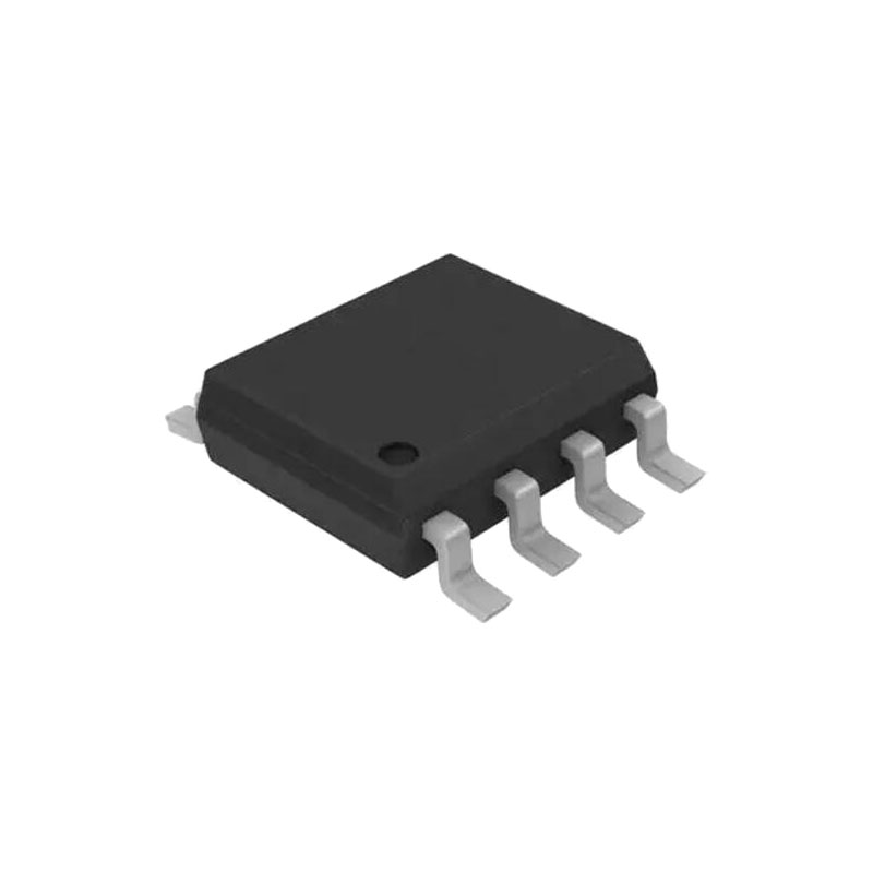
The MAX629’s combination of low supply current, logic controlled shutdown, small package, and tiny external components makes it an extremely compact and efficient high-voltage biasing solution that’s ideal for battery-powered applications. The MAX629 is available in an 8-pin SO package.
Applications
● Positive or Negative LCD Bias Generators
● High-Efficiency DC-DC Boost Converters
● Varactor Tuning Diode Bias
● Palmtop Computers
● 2-Cell and 3-Cell Battery-Powered Applications
Features
● Internal, 500mA, 28V N-Channel Switch (No External FET Required)
● Generates Positive or Negative Output Voltages
● 80μA Supply Current
● 1μA Max Shutdown Current
● Up to 300kHz Switching Frequency
● Adjustable Current Limit Allows Use of Small, Inexpensive Inductors
● 8-Pin SO Package
Detailed Description
The MAX629 low-power, boost DC-DC converter provides either positive or negative output voltages up to ±28V from a wide range of input voltages. It is designed primarily for use in low-power, high-voltage applications such as LCD biasing and set-top box varactor tuning. The MAX629’s unique control scheme provides high efficiency and a wide range of output voltages with only 80μA quiescent supply current, making it ideal for battery-powered applications. The internal N-channel DMOS switch has a pin-programmable current limit (250mA and 500mA), allowing optimization of output current and component size.
Control Scheme
A combination of peak-current limiting and a pair of oneshots controls the MAX629 switching, determining the maximum on-time and constant off-time. During the oncycle, the internal switch closes, and current through the inductor ramps up until either the fixed 10μs maximum on-time expires (at low input voltages) or the switch’s peak current limit is reached. The peak switch current limit is selectable to either 500mA (ISET = VCC) or 250mA (ISET = GND) (see Setting the Current Limit). After the on-cycle terminates, the switch turns off, charging the output capacitor through the diode. In normal operation, the minimum off-time is set to 1μs for positive output voltages and 3.5μs for negative output voltages. When the output is well below regulation, however, the off-time is increased to 5μs to provide soft-start during start-up. The switching frequency, which depends upon the load, can be as high as 300kHz.
Setting the Current Limit
External current-limit selection provides added control over the MAX629’s output performance. A higher current limit increases the amount of energy stored in the inductor during each cycle, which provides a higher output current capability. For higher output current applications, choose the 500mA current-limit option by connecting ISET to VCC. When lower output current is required, the 250mA current limit can provide several advantages. First, a smaller inductor can be used, which saves board area and cost. Second, the smaller energy transfer per cycle reduces output ripple for a given capacitor, providing design flexibility between board area, cost, and output ripple by allowing cheaper, higher-ESR capacitors. Connect ISET to GND to select the 250mA current-limit option.
Inductor Selection
The MAX629’s high switching frequency allows for the use of a small inductor. The 47μH inductor shown in the Typical Operating Circuit is recommended for most applications. Larger inductances reduce the peak inductor current, but may limit output current capability at low input voltages and provide slower start-up times. Smaller inductances require less board space, but may cause greater peak current due to current-sense comparator propagation delay. If input voltages below 2V will be common, reducing the inductance to 22μH might improve performance; however, maximum load current and efficiency may decline. It is important to thoroughly test operation under all input and output conditions to ensure proper component selection.

