DESCRIPTION
The LTC2262-14 is a sampling 14-bit A/D converter designed for digitizing high frequency, wide dynamic range signals. The LTC2262-14 is perfect for demanding communications applications with AC performance that includes 72.8dB SNR and 88dB spurious free dynamic range (SFDR). Ultralow jitter of 0.17psRMS allows undersampling of IF frequencies with excellent noise performance. DC specs include ±1LSB INL (typical), ±0.3LSB DNL (typical) and no missing codes over temperature. The transition noise is a low 1.2LSBRMS. The digital outputs can be either full rate CMOS, double data rate CMOS, or double data rate LVDS. A separate output power supply allows the CMOS output swing to range from 1.2V to 1.8V. The ENC+ and ENC– inputs may be driven differentially or single ended with a sine wave, PECL, LVDS, TTL or CMOS inputs. An optional clock duty cycle stabilizer allows high performance at full speed for a wide range of clock duty cycles.
FEATURES
72.8dB SNR
88dB SFDR
Low Power: 149mW
Single 1.8V Supply
CMOS, DDR CMOS or DDR LVDS Outputs
Selectable Input Ranges: 1VP-P to 2VP-P
800MHz Full-Power Bandwidth S/H
Optional Data Output Randomizer
Optional Clock Duty Cycle Stabilizer
Shutdown and Nap Modes
Serial SPI Port for Configuration
Pin Compatible 14-Bit and 12-Bit Versions
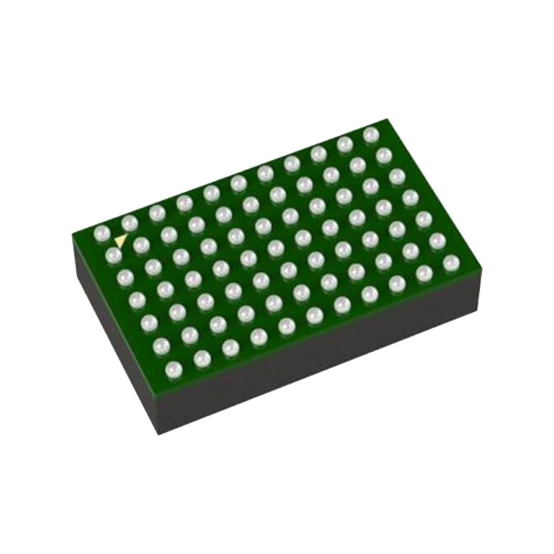
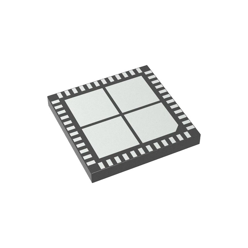
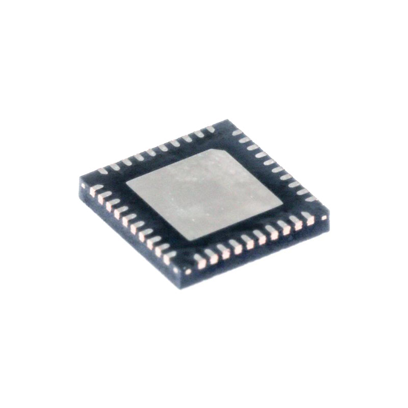
40-Pin (6mm × 6mm) QFN Package
APPLICATIONS
DESCRIPTION
14-Bit, 150Msps Ultralow Power 1.8V ADC
Communications
Cellular Base Stations
Software Defined Radios
Portable Medical Imaging
Multi-Channel Data Acquisition
Nondestructive Testing
APPLICATIONS INFORMATION
CONVERTER OPERATION
The LTC2262-14 is a low power 14-bit 150Msps A/D converter that is powered by a single 1.8V supply. The analog inputs should be driven differentially. The encode input can be driven differentially, or single ended for lower power consumption. The digital outputs can be CMOS, double data rate CMOS (to halve the number of output lines), or double data rate LVDS (toreduce digital noise in the system.) Many additional features can be chosen by programming the mode control registers through a serial SPI port. See the Serial Programming Mode section.
ANALOG INPUT
The analog input is a differential CMOS sample-and-hold circuit. The inputs should be driven differentially around a common mode voltage set by the VCM output pin, which is nominally VDD/2. For the 2V input range, the inputs should swing from VCM – 0.5V to VCM + 0.5V. There
should be 180° phase difference between the inputs.
INPUT DRIVE CIRCUITS
Input filtering
If possible, there should be an RC lowpass filter right at the analog inputs. This lowpass filter isolates the drive circuitry from the A/D sample-and-hold switching, and also limits wideband noise from the drive circuitry. The RC component values should be chosen based on the application’s input frequency.
Transformer Coupled Circuits
The center tap is biased with VCM, setting the A/D input at its optimal DC level. At higher input frequencies a transmission line balun transformer (Figures 4 to 6) has better balance, resulting in lower A/D distortion.
Encode Input
The signal quality of the encode inputs strongly affects the A/D noise performance. The encode inputs should be treated as analog signals—do not route them next to digital traces on the circuit board. There are two modes of operation for the encode inputs: the differential encode mode and the single-ended encode mode The differential encode mode is recommended for sinusoidal, PECL or LVDS encode inputs. The encode inputs are internally biased to 1.2V through 10k equivalent resistance. The encode inputs can be taken above VDD (up to 3.6V), and the common mode range is from 1.1V to 1.6V. In the differential encode mode, ENC– should stay at least 200mV above ground to avoid falsely triggering the single-ended encode mode. For good jitter performance ENC+ and ENC– should have fast rise and fall times.