BESCHREIBUNG
The LTC4362 monolithic overvoltage/overcurrent protector safeguards 2.5V to 5.5V systems from power supply overvoltage. It is designed for portable devices with multiple power supply options including wall adaptors, car battery adaptors and USB ports.
The LTC4362 controls an internal 40mΩ N-channel MOSFET in series with the input power supply. During overvoltage transients, the LTC4362 turns off the MOSFET within 1µs, isolating downstream components from the input supply. In most applications, the LTC4362 rides through inductive cable transients without requiring transient voltage suppressors or other external components. An internal current sense resistor is used to implement overcurrent protection.
The LTC4362 has a delayed start-up at plug-in and controlled dV/dt ramp-up for inrush current limiting. A PWRGD pin provides power good monitoring for VIN. The LTC4362 features a soft-shutdown controlled by the ON pin and drives an optional external P-channel MOSFET for negative voltage protection. Following an overvoltage condition, the LTC4362 automatically restarts with a 130ms delay. After an overcurrent fault, the LTC4362-1 remains off while the LTC4362-2 automatically restarts after a 130ms delay.
FEATURES
2.5V to 5.5V Operation
Overvoltage Protection Up to 28V
Internal 40mΩ N-Channel MOSFET and 31mΩ RSENSE
Avalanche Rated MOSFET Requires No Input Capacitor or TVS for Most Applications
<1µs Overvoltage Turn-Off, Gentle Shutdown
2% Accurate 5.8V Overvoltage Threshold
20% Accurate 1.5A Overcurrent Threshold
Input Withstands Up to ±25kV HBM ESD with ≥1µF COUT
Controlled Power-Up dV/dt Limits Inrush Current
Reverse Voltage Protection Driver
Low Current Shutdown
Latchoff (LTC4362-1) or Auto-Retry (LTC4362-2) After Overcurrent
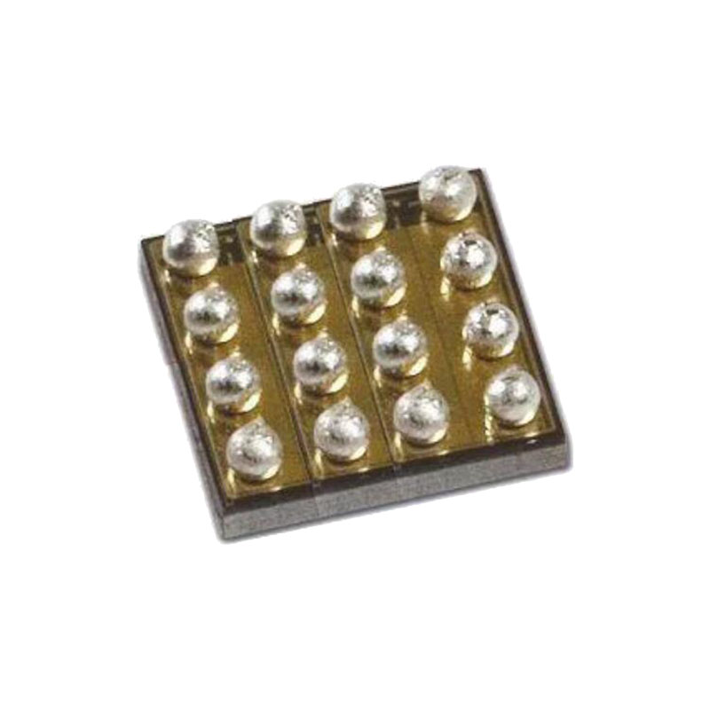
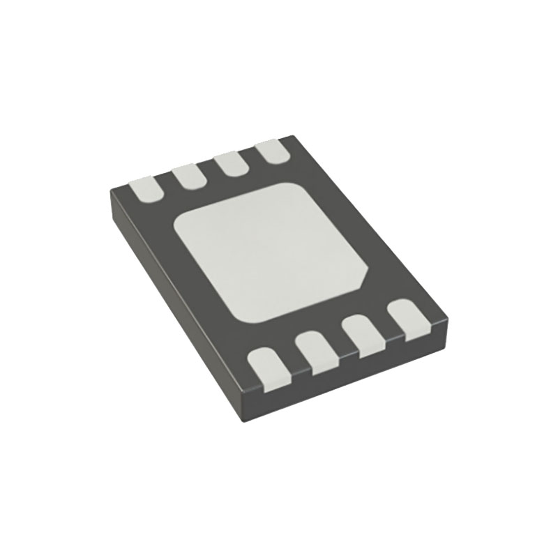
Available in 8-Lead DFN 2mm × 3mm Package
ANWENDUNGEN
USB Protection
Handheld Computers
Cell/Smart Phones
MP3/MP4 Players
Digital Cameras
OPERATION
Mobile devices like cell phones and MP3/MP4 players have highly integrated subsystems fabricated from deep submicron CMOS processes. The small form factor is accompanied by low absolute maximum voltage ratings. The sensitive electronics are susceptible to damage from transient or DC overvoltage conditions from the power supply.
Failures or faults in the power adaptor can cause an overvoltage event. So can hot-plugging an AC adaptor into the power input of the mobile device (see Application Note 88). Today’s mobile devices derive their power supply or recharge their internal batteries from multiple alternative inputs like AC wall adaptors, car battery adaptors and USB ports. A user might unknowingly plug in the wrong adaptor, damaging the device with a high or even a negative power supply voltage.
The LTC4362 protects low voltage electronics from these overvoltage conditions by controlling an internal N-channel MOSFET configured as a pass transistor. At power-up (VIN > 2.1V), a start-up delay cycle begins. Any overvoltage condition causes the delay cycle to continue until a safe voltage is present. When the delay cycle completes, an internal high-side switch driver slowly ramps up the MOSFET gate, powering up the output at a controlled rate and limiting the inrush current to the output capacitor.If the voltage at the IN pin exceeds 5.8V (VIN(OV)), the internal N-channel MOSFET is turned off quickly to protect the load. The incoming power supply must remain below 5.7V (VOUT(OV) – ∆VOV) for the duration of the start-up delay to restart the OUT ramp-up.
An internal sense resistor is used to implement an overcurrent protection with a 1.5A current trip threshold and a 10µs glitch filter. After an overcurrent, the LTC4362-1 latches off while the LTC4362-2 restarts following a 130ms delay.
The LTC4362 has a CMOS compatible ON input. When driven low, the part is enabled. When driven high, the internal N-channel MOSFET is turned off and the supply current of the LTC4362 drops to 1.5μA. The PWRGD pull-down releases during this low current sleep mode, UVLO, overvoltage, overcurrent or thermal shutdown and the subsequent 130ms start-up delay. After the start-up delay, the internal MOSFET gate starts its 3V/ms ramp-up. It trips an internal gate high threshold to trigger a 65ms delay. When that completes, PWRGD pulls low. The output pull-down device is capable of sinking up to 3mA allowing it to drive an optional LED. The LTC4362 has a GATEP pin that drives an optional external P-channel MOSFET to provide protection against negative voltages at IN.