BESCHREIBUNG
Der hot-swap-fähige 2-Draht-Buspuffer LTC4307 ermöglicht das Einstecken von E/A-Karten in eine stromführende Backplane ohne Beeinträchtigung der Daten- und Taktbusse. Der LTC4307 bietet eine bidirektionale Pufferung, so dass die Kapazitäten der Backplane und der Karte isoliert bleiben. Dank der niedrigen Offset- und hohen VOL-Toleranz können mehrere Bausteine auf den Takt- und Datenbussen kaskadiert werden. Wenn SDAOUT oder SCLOUT für 30ms auf Low liegen, unterbricht der LTC4307 automatisch die Busverbindung. Zu diesem Zeitpunkt erzeugt der LTC4307 automatisch bis zu 16 Taktimpulse auf SCLOUT, um zu versuchen, den Bus zu befreien. Die Verbindung wird wiederhergestellt, wenn der blockierte Bus wieder frei ist.
Während der Einfügung werden die SDA- und SCL-Leitungen auf 1V vorgeladen, um Busstörungen zu minimieren. Wenn der ENABLE-Eingang auf High geschaltet wird, kann der LTC4307 nach einem Stopbit oder Busleerlauf eine Verbindung herstellen. Wenn Sie ENABLE auf Low schalten, wird die Verbindung zwischen SDAIN und SDAOUT, SCLIN und SCLOUT unterbrochen. READY ist ein Open-Drain-Ausgang, der anzeigt, dass die Backplane und die Kartenseite verbunden sind.
FEATURES
Bidirektionaler Puffer mit Stuck Bus Recovery
60mV Puffer-Offset unabhängig von der Last
30ms Stuck Bus Timeout
Kompatibel mit nicht-kompatiblen VOL I2C Geräten
Verhindert die Beschädigung von SDA und SCL beim Einsetzen und Entfernen der Platine unter Spannung
±5kV Human Body Model ESD-Schutz
Isoliert die Eingangsleitung SDA und SCL vom Ausgang
Kompatibel mit I2CTM, I2C Fast Mode und SMBus
READY Open-Drain Ausgang
1V Vorladung auf allen SDA- und SCL-Leitungen
Hochohmige SDA, SCL Pins für VCC = 0V
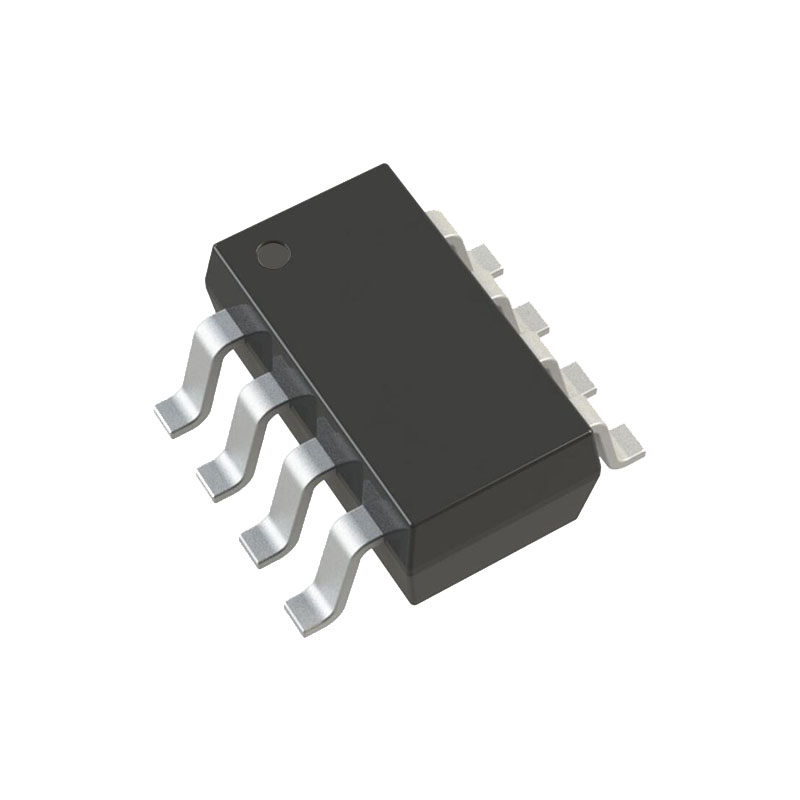
Kleine 8-polige (3mm × 3mm) DFN- und 8-polige MSOP-Gehäuse
APPLICATIOS
Live Board einfügen
Server
Kapazitätspuffer/Bus Extender
RAID-Systeme
ATCA
OPERATION
Start-up
Wenn der LTC4307 zum ersten Mal Strom an seinem VCC-Pin erhält, entweder beim Einschalten oder beim Einschalten unter Spannung, geht er in einen Unterspannungs-Lockout-Zustand (UVLO) über und ignoriert jegliche Aktivität an den SDA- oder SCL-Pins, bis VCC über 2V (typ.) ansteigt. Damit wird sichergestellt, dass der LTC4307 nicht versucht zu funktionieren, bevor er nicht über eine ausreichende Spannung verfügt.
Anschluss Schaltungen
Sobald die Verbindungsschaltung aktiviert ist, ist die Funktionalität der Pins SDAIN und SDAOUT identisch. Wenn einer der beiden Pins zu einem beliebigen Zeitpunkt auf Low gezwungen wird, sind beide Pins auf Low. Der LTC4307 ist tolerant gegenüber logischen Low-Spannungen auf dem I2C-Bus bis zur 0,3VCC VIL I2C-Spezifikation. Wenn der LTC4307 eine steigende Flanke auf dem Bus erkennt, deaktiviert er seine Pull-Down-Bausteine für Busspannungen von bis zu 0,48V und aktiviert seine Beschleuniger. Diese Methode maximiert die Effektivität der Anstiegszeit-Beschleunigerschaltung und gewährleistet die Kompatibilität mit den anderen Bausteinen der LTC4300-Buspufferfamilie. Es ist darauf zu achten, dass Bausteine, die an der Taktverlängerung oder Arbitrierung teilnehmen, an den Eingängen des LTC4307 logisch niedrige Spannungen unter 0,48V erzwingen.
Ausbreitungsverzögerungen
Während einer steigenden Flanke wird die Anstiegszeit auf jeder Seite durch den Bus-Pull-up-Widerstand und die äquivalente Kapazität auf der Leitung bestimmt. Wenn die Pull-up-Widerstände gleich sind, entsteht ein Unterschied in der Anstiegszeit, der direkt proportional zum Unterschied in der Kapazität zwischen den beiden Seiten ist. Dieser Effekt ist in Abbildung 2 für VCC = 5,5V und einen 10k Pull-up-Widerstand auf jeder Seite dargestellt (50pF auf der einen Seite und 150pF auf der anderen). Da die Ausgangsseite eine geringere Kapazität hat als die Eingangsseite, steigt sie schneller an und die effektive Ausbreitungsverzögerung ist negativ.
ANWENDUNGSINFORMATIONEN
Live-Insertion und Kapazitätspufferung Anwendung
Der LTC4307, die die Hot SwapTM -, Kapazitätspufferungs- und Vorladefunktionen des LTC4307 nutzen. Wenn die E/A-Karten ohne den LTC4307 direkt auf die Backplane gesteckt werden
Puffer würden sich alle Kapazitäten der Backplane und der Karte direkt addieren, so dass die Anforderungen an die Anstiegs- und Abfallzeit nur schwer zu erfüllen wären. Durch die Platzierung eines LTC4307 an der Kante jeder Karte wird die Kartenkapazität jedoch von der Backplane isoliert. Bei einer bestimmten E/A-Karte steuert der LTC4307 die Kapazität aller Komponenten auf der Karte und die Backplane muss nur die Kapazität des LTC4307 steuern, die weniger als 10pF beträgt.