FEATURES
► Ultrawideband frequency range: 100 MHz to 60 GHz
► Reflective design
► Bond pads for wire bond and ribbon bond
► Low insertion loss
► 1.0 dB typical up to 18 GHz
► 1.3 dB typical up to 44 GHz
► 1.5 dB typical up to 55 GHz
► High input linearity
► P1dB: 28 dBm typical
► IP3: 50 dBm typical
► High RF power handling
► Through path: 27 dBm up to 40 GHz
► Hot switching: 27 dBm up to 40 GHz
► No low frequency spurious signals
► RF settling time (50% VCTRL to 0.1 dB of final RF output): 17 ns
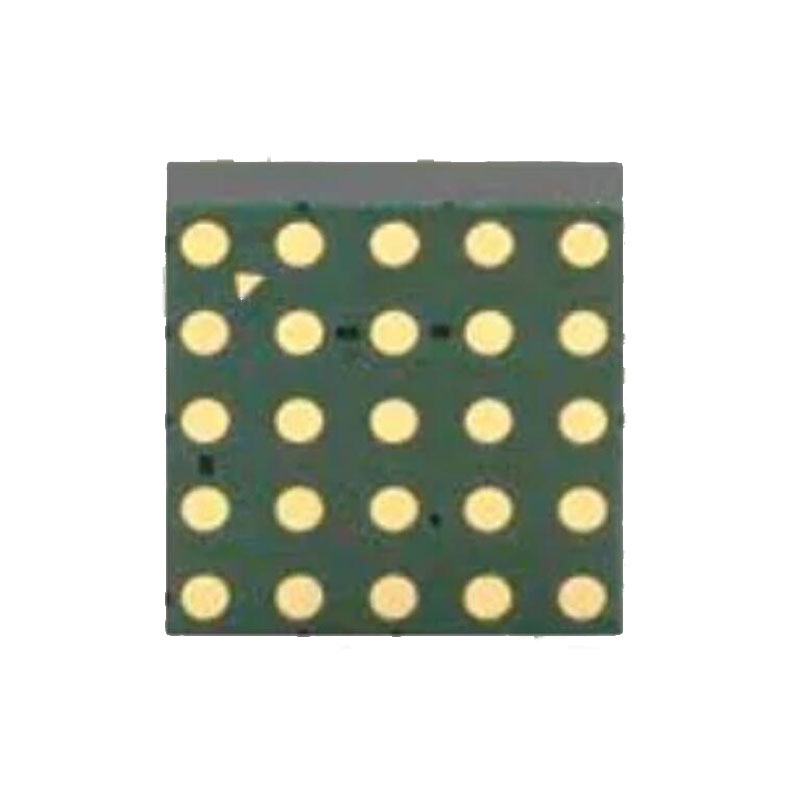
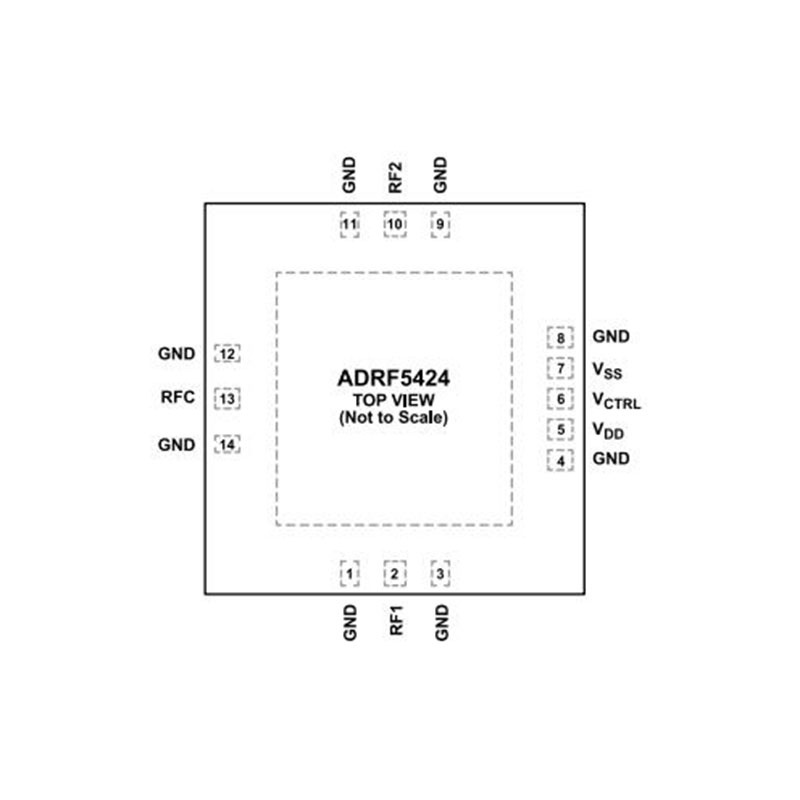
► 14-pad, 2.571 mm × 2.471 mm, die on carrier [CHIP]
ANWENDUNGEN
► Test and instrumentation
► Cellular infrastructure: 5G mmWave
► Military radios, radars, and electronic counter measures (ECMs)
► Microwave radios and very small aperture terminals (VSATs)
ALLGEMEINE BESCHREIBUNG
The ADRF5424 is a reflective, single-pole double-throw (SPDT) switch manufactured in a silicon process attached on a gallium arsenide (GaAs) carrier substrate. The substrate incorporates the bond pads for chip and wire assembly, and the bottom of the device is metalized, connected to ground.
This device operates from 100 MHz to 60 GHz with better than 1.5 dB of insertion loss and 35 dB of isolation at 55 GHz. The ADRF5424 has an RF input power handling capability of 27 dBm up to 40 GHz for both the through path and hot switching.
The ADRF5424 draws a low current of 14 µA on the positive supply of +3.3 V and 120 µA on negative supply of −3.3 V. The device features complementary metal-oxide semiconductor (CMOS)-/low voltage transistor to transistor logic (LVTTL)-compatible controls.
The ADRF5424 is designed to match a characteristic impedance of 50 Ω.
ARBEITSTHEORIE
The ADRF5424 integrates a driver to perform logic functions inter nally and provides the user with the advantage of a simplified CMOS-/LVTTL-compatible control interface. This driver features a single digital control input pad, VCTRL. The logic level applied to the VCTRL pad determines which RF port is in the insertion loss state and in the isolation state. The unselected RF port of the ADRF5424 is reflective. The isolation path provides high isolation between the unselected port and the insertion loss path.
RF-EINGANG UND -AUSGANG
All of the RF ports (RFC, RF1, and RF2) are dc-coupled to 0 V, and no dc blocking is required at the RF ports when the RF line potential is equal to 0 V.
STROMVERSORGUNG
The ADRF5424 requires a positive supply voltage applied to the VDD pad and a negative supply voltage applied to the VSS pad. Bypassing capacitors are recommended on the supply lines to filter high frequency noise.
Die ideale Einschaltsequenz ist wie folgt:
- Verbinden Sie mit GND.
- Power up the VDD and VSS voltages. Power up VSS after VDD to avoid current transients on VDD during ramp up.
- Power up the digital control inputs. The order of the digital control inputs before the VDD voltage supply can inadvertently forward bias and damage the internal ESD protection structures. To avoid this damage, use a series 1 kΩ resistor to limit the current flowing into the control pad. Use pull-up or pull-down resistors if the controller output is in a high impedance state after the VDD voltage is powered up and the control pads are not driven to a valid logic state.
- Apply an RF input signal to RFC, RF1, or RF2.
The ideal power-down sequence is the reverse order of the power up sequence.
ANWENDUNGSINFORMATIONEN
DIE ASSEMBLY
The ADRF5424 is designed to have the optimum RF input and output impedance match with 2 mil x 0.5 mil gold ribbon wire and typical 3 mil loop height. Alternatively, using multiple wire bonds with equivalent inductance yields similar performance. For RF rout ing from the device, coplanar waveguide or microstrip transmission lines can be used. No impedance matching is required on the transmission line pad because the device is designed to match internally the recommended ribbon bond. A spacing of 3 mils from the RF transmission line to the device edge is recommended for optimum performance.