BESCHREIBUNG
The LTC3786 is a high performance synchronous boost converter controller that drives all N-channel power MOSFETs. Synchronous rectification increases efficiency, reduces power losses and eases thermal requirements, allowing the LTC3786 to be used in high power boost applications.
A 4.5V to 38V input supply range encompasses a wide range of system architectures and battery chemistries. When biased from the output of the boost converter or another auxiliary supply, the LTC3786 can operate from an input supply as low as 2.5V after start-up. The 55µA no-load quiescent current extends operating run time in battery-powered systems.
The operating frequency can be set for a 50kHz to 900kHz range or synchronized to an external clock using the internal PLL. The LTC3786 also features a precision 1.2V reference and a power good output indicator. The SS pin ramps the output voltage during start-up. The PLLIN/MODE pin selects among Burst Mode® operation, pulse-skipping mode or continuous inductor current mode at light loads.
FEATURES
Synchronous Operation For Highest Efficiency and Reduced Heat Dissipation
Wide VIN Range: 4.5V to 38V (40V Abs Max) and Operates Down to 2.5V After Start-Up
Output Voltages Up to 60V
±1% 1.2V Reference Voltage
RSENSE or Inductor DCR Current Sensing
100% Duty Cycle Capability for Synchronous MOSFET
Low Quiescent Current: 55µA
Phase-Lockable Frequency (75kHz to 850kHz)
Programmable Fixed Frequency (50kHz to 900kHz)
Adjustable Output Voltage Soft-Start
Power Good Output Voltage Monitor
Low Shutdown Current IQ: <8µA
Internal 5.4V LDO for Gate Drive Supply
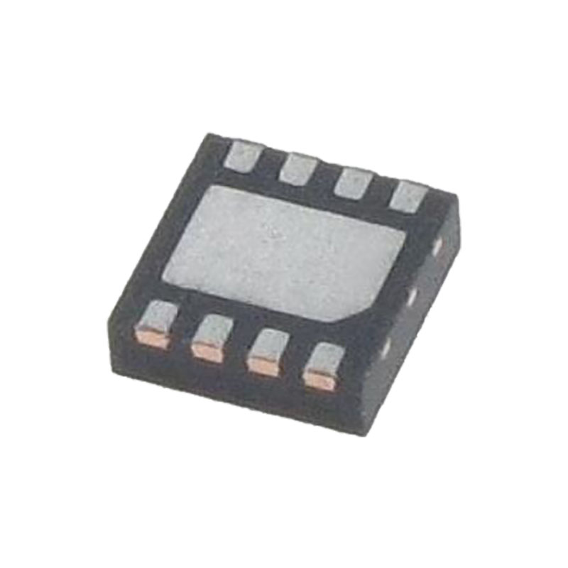
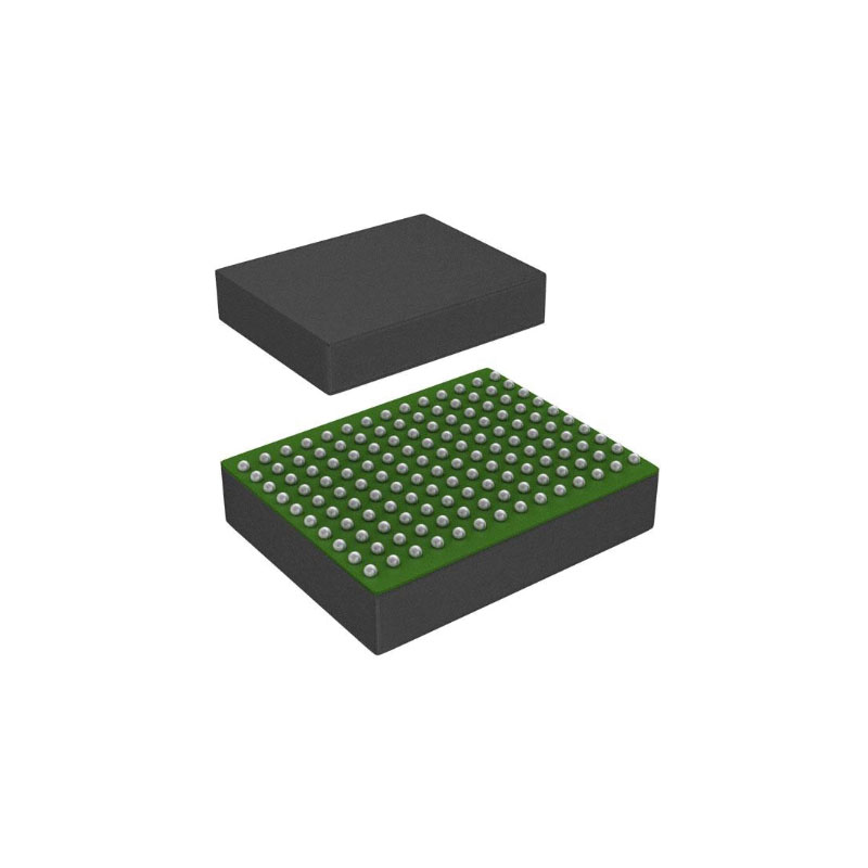
Thermally Enhanced 16-Pin 3mm × 3mm QFN and MSOP Packages
AEC-Q100 qualifiziert für Automobilanwendungen
ANWENDUNGEN
Industrielle und automobile Stromversorgungen
Automotive Start-Stop Systems
Medizinische Geräte
High Voltage Battery-Powered Systems
OPERATION
Hauptkontrollschleife
The LTC3786 uses a constant-frequency, current mode step-up control architecture. During normal operation, the external bottom MOSFET is turned on when the clock sets the RS latch, and is turned off when the main current comparator, ICMP , resets the RS latch. The peak inductor current at which ICMP trips and resets the latch is controlled by the voltage on the ITH pin, which is the output of the error amplifier, EA. The error amplifier compares the output voltage feedback signal at the VFB pin, (which is generated with an external resistor divider connected across the output voltage, VOUT , to ground) to the internal 1.200V reference voltage. In a boost converter, the required inductor current is determined by the load current, VIN and VOUT . When the load current increases, it causes a slight decrease in VFB relative to the reference, which causes the EA to increase the ITH voltage until the average inductor current in each channel matches the new requirement based on the new load current.
After the bottom MOSFET is turned off each cycle, the top MOSFET is turned on until either the inductor current starts to reverse, as indicated by the current comparator IREV, or the beginning of the next clock cycle.
Shutdown and Start-Up (RUN and SS Pins)
The LTC3786 can be shut down using the RUN pin. Pulling this pin below 1.28V shuts down the main control loop. Pulling this pin below 0.7V disables the controller and most internal circuits, including the INTVCC LDOs. In this state, the LTC3786 draws only 8µA of quiescent current. Note: Do not apply load while the chip is in shutdown. The output MOSFET will be turned off during shutdown and the output load may cause excessive power dissipation in the body diode.
The start-up of the controller’s output voltage, VOUT , is controlled by the voltage on the SS pin. When the voltage on the SS pin is less than the 1.2V internal reference, the LTC3786 regulates the VFB voltage to the SS pin voltage instead of the 1.2V reference. This allows the SS pin to be used to program a soft-start by connecting an external capacitor from the SS pin to GND. An internal 10µA pullup current charges this capacitor creating a voltage ramp on the SS pin. As the SS voltage rises linearly from 0V to 1.2V, the output voltage rises smoothly to its final value.