FEATURES
► Single 8-, 10-, 12-bit DACs, 2 LSB INL
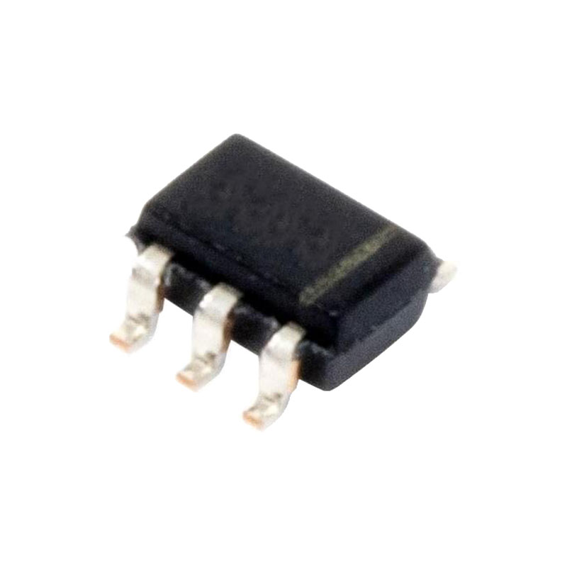
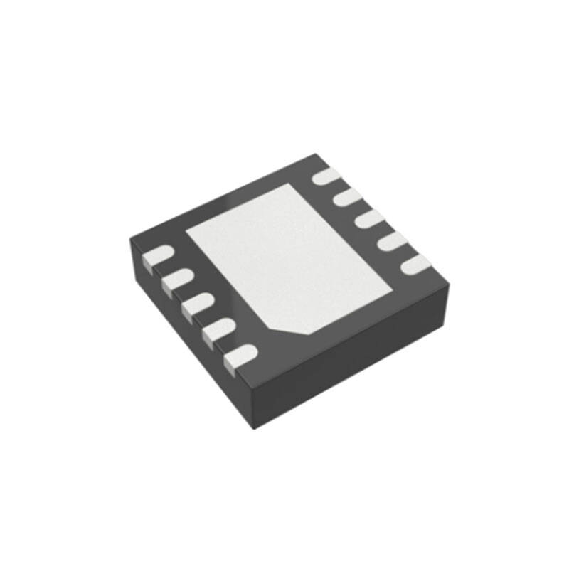
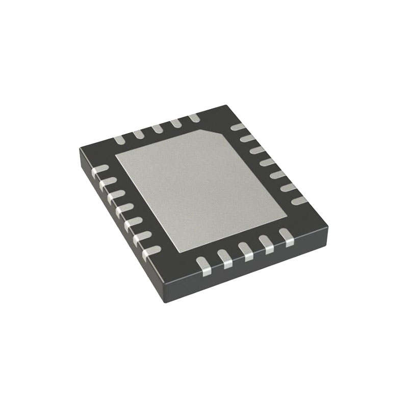
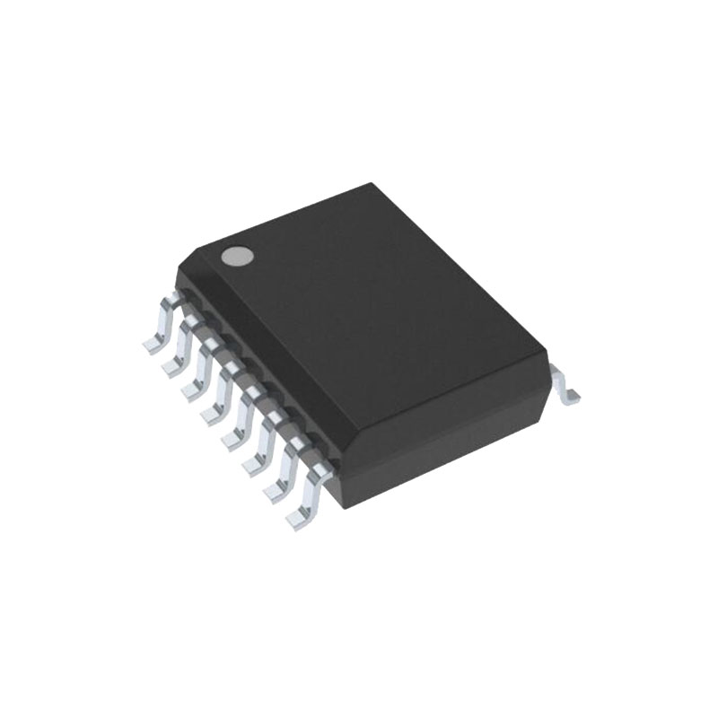
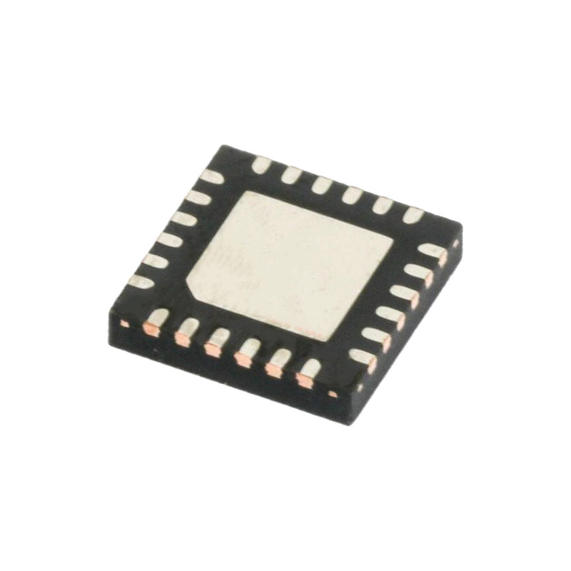
► 6-lead LFCSP and SC70 packages
► Micropower operation: 100 µA maximum at 5 V
► Power down to <150 nA at 3 V
► 2.7 V to 5.5 V power supply
► Guaranteed monotonic by design
► Power-on reset to 0 V with brownout detection
► 3 power-down functions
► I2C compatible serial interface supports standard (100 kHz), fast (400 kHz), and high speed (3.4 MHz) modes
► On-chip output buffer amplifier, rail-to-rail operation
► AEC-Q100 qualified for automotive applications
ANWENDUNGEN
► Process control
► Data acquisition systems
► Portable battery-powered instruments
► Digital gain and offset adjustment
► Programmable voltage and current sources
► Programmable attenuators
ALLGEMEINE BESCHREIBUNG
The AD5602/AD5612/AD5622, members of the nanoDAC® family, are single 8-, 10-, 12-bit buffered voltage-out digital-to-analog converters (DAC) that operate from a single 2.7 V to 5.5 V supply, consuming
The AD5602/AD5612/AD5622 use a 2-wire I2C compatible serial interface that operates in standard (100 kHz), fast (400 kHz), and high speed (3.4 MHz) modes.
The references for AD5602/AD5612/AD5622 derive from the power supply inputs to give the widest dynamic output range. Each device incorporates a power-on reset circuit that ensures the DAC output powers up to 0 V and remains there until a valid write takes place to the device. The devices contain a power-down feature that reduces the current consumption of the devices to <150 nA at 3 V and provides software selectable output loads while in power-down mode. The devices are put into power-down mode over the serial interface. The low power consumption of the AD5602/AD5612/AD5622 in normal operation makes them ideally suited for use in portable, battery operated equipment. The typical power consumption is 0.4 mW at 5 V.
PRODUKT-HIGHLIGHTS
- Available in 6-lead LFCSP and SC70 packages.
- Maximum 100 µA power consumption, single-supply operation.These devices operate from a single 2.7 V to 5.5 V supply,typically consuming 0.2 mW at 3 V and 0.4 mW at 5 V, making them ideal for battery-powered applications.
- The on-chip output buffer amplifier allows the output of the DAC to swing rail-to-rail with a typical slew rate of 0.5 V/µs.
- Reference derived from the power supply.
- Standard, fast, and high speed mode I2C interface.
- Designed for very low power consumption.
- Power-down capability. When powered down, the DAC typically consumes <150 nA at 3 V.
- Power-on reset and brownout detection.
SERIAL INTERFACE
The AD5602/AD5612/AD5622 have 2-wire I2C compatible serial interfaces. The AD5602/AD5612/ AD5622 can be connected to an I2C bus as a target device, under the control of a controller device.
The AD5602/AD5612/AD5622 support standard (100 kHz), fast (400 kHz), and high speed (3.4 MHz) data transfer modes. Support is not provided for 10 bit addressing and general call addressing.
The AD5602/AD5612/AD5622 each have a 7-bit target address. The five most significant bits (MSB) are 00011 and the two LSBs are determined by the state of the ADDR pin. The facility to make hardwired changes to ADDR allows the user to incorporate up to three of these devices on one bus.
The 2-wire serial bus protocol operates as follows:
- The controller initiates data transfer by establishing a start condition, which is when a high to low transition on the SDA line occurs while SCL is high. The following byte is the address byte, which consists of the 7-bit target address. The target address corresponding to the transmitted address responds by pulling SDA low during the ninth clock pulse (this is termed the acknowledge bit). At this stage, all other devices on the bus remain idle while the selected device waits for data to be written to, or read from, its shift register.
- Data is transmitted over the serial bus in sequences of nine clock pulses (eight data bits followed by an acknowledge bit). The transitions on the SDA line must occur during the low period of SCL and remain stable during the high period of SCL.
- When all data bits have been read or written, a stop condition is established. In write mode, the controller pulls the SDA line high during the 10th clock pulse to establish a stop condition. If a stop condition is generated between the 7th and 8th clock pulse of the I2C address frame, a power cycle is required to recover the device. In read mode, the controller issues a no acknowledge for the ninth clock pulse (that is, the SDA line remains high). The controller then brings the SDA line low before the 10th clock pulse, and then high during the 10th clock pulse to establish a stop condition.
