ALLGEMEINE BESCHREIBUNG
The AD829 is a low noise (1.7 nV/√Hz), high speed op amp with custom compensation that provides the user with gains of 1 to 20 while maintaining a bandwidth >50 MHz. Its 0.04° differential phase and 0.02% differential gain performance at 3.58 MHz and 4.43 MHz, driving reverse-terminated 50 Ω or 75 Ω cables, makes it ideally suited for professional video applications. The AD829 achieves its 230 V/µs uncompensated slew rate and 750 MHz gain bandwidth while requiring only 5 mA of current from power supplies.
The external compensation pin of the AD829 gives it exceptional versatility. For example, compensation can be selected to optimize the bandwidth for a given load and power supply voltage. As a gain-of-2 line driver, the −3 dB bandwidth can be increased to 95 MHz at the expense of 1 dB of peaking. Its output can also be clamped at its external compensation pin.
The AD829 exhibits excellent dc performance. It offers a minimum open-loop gain of 30 V/mV into loads as low as 500 Ω, a low input voltage noise of 1.7 nV/√Hz, and a low input offset voltage of 1 mV maximum. Common-mode rejection and power supply rejection ratios are both 120 dB.
This op amp is also useful in multichannel, high speed data conversion where its fast (90 ns to 0.1%) settling time is important. In such applications, the AD829 serves as an input buffer for 8-bit to 10-bit ADCs and as an output I/V converter for high speed DACs.
Operating as a traditional voltage feedback amplifier, the AD829 provides many of the advantages that a transimpedance amplifier offer. A bandwidth >50 MHz can be maintained for a range of gains through the replacement of the external compensation capacitor. The AD829 and the transimpedance amplifier are both unity-gain stable and provide similar voltage noise performance (1.7 nV/√Hz); however, the current noise of the AD829 (1.5 pA/√Hz) is less than 10% of the noise of transimpedance amplifiers. The inputs of the AD829 are symmetrical.
FEATURES
High speed
120 MHz bandwidth, gain = −1
230 V/µs slew rate
90 ns settling time to 0.1%
Ideal for video applications
0.02% differential gain
0.04° differential phase
Low noise
1.7 nV/√Hz input voltage noise
1.5 pA/√Hz input current noise
Excellent dc precision
1 mV maximum input offset voltage (over temperature)
0.3 µV/°C input offset drift
Flexible operation
Specified for ±5 V to ±15 V operation
±3 V output swing into a 150 Ω load
External compensation for gains 1 to 20
5 mA supply current
Available in tape and reel in accordance with EIA-481A standard
PRODUKT-HIGHLIGHTS
1.The input voltage noise of 2 nV/√Hz, current noise of 1.5 pA/√Hz, and 50 MHz bandwidth for gains of 1 to 20 make the AD829 an ideal preamp.
2. A differential phase error of 0.04 and a 0.02% differential gain error, at the 3.58 MHz NTSC, 4.43 MHz PAL, and SECAM color subcarrier frequencies, make the op amp an outstanding video performer for driving reverse-terminated 50 Ω and 75 Ω cables to ±1 V (at their terminated end).
3.The AD829 can drive heavy capacitive loads.
4.Performance is fully specified for operation from ±5 V to ±15 V supplies.
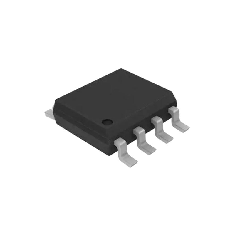
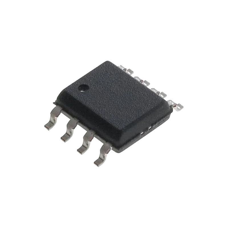
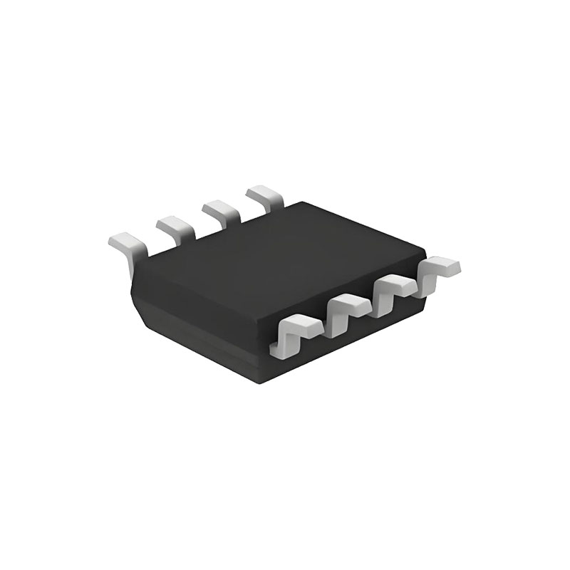
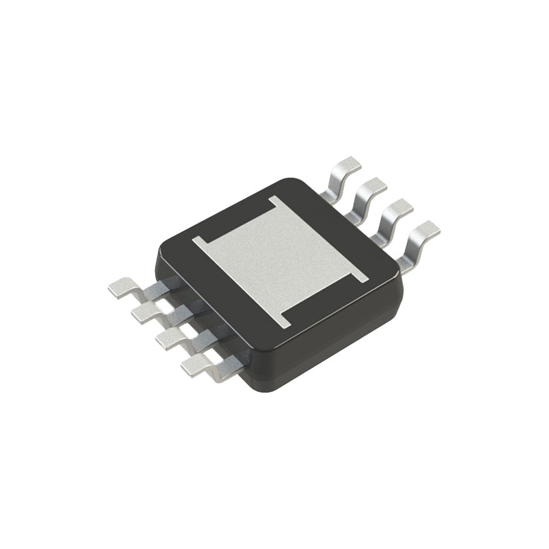
5. The AD829 is available in PDIP, CERDIP, and small outline packages. Chips and MIL-STD-883B parts are also available. The 8-lead SOIC is available for the extended temperature range (−40°C to +125°C).
EXTERNALLY COMPENSATING THE AD829
The AD829 is stable with no external compensation for noise gains greater than 20. For lower gains, two different methods of frequency compensating the amplifier can be used to achieve closed-loop stability: shunt and current feedback compensation.

