ALLGEMEINE BESCHREIBUNG
The AD8418A is a high voltage, high resolution current shunt amplifier. It features an initial gain of 20 V/V, with a maximum ±0.15% gain error over the entire temperature range. The buffered output voltage directly interfaces with any typical converter. The AD8418A offers excellent input common-mode rejection from −2 V to +70 V. The AD8418A performs bidirectional current measurements across a shunt resistor in a variety of automotive and industrial applications, including motor control, power management, and solenoid control.
The AD8418A offers breakthrough performance throughout the −40°C to +150°C temperature range. It features a zero drift core, which leads to a typical offset drift of 0.1 μV/°C throughout the operating temperature range and the common-mode voltage range. The AD8418A is qualified for automotive applications.
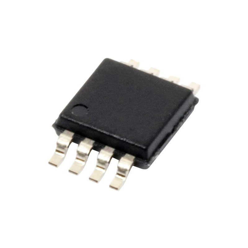
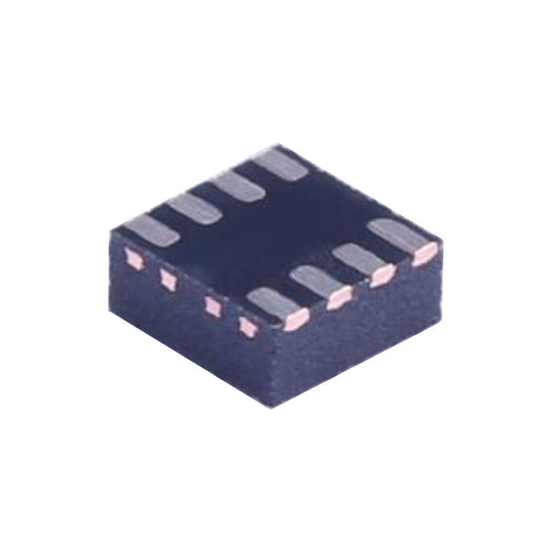
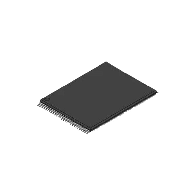
The device includes EMI filters and patented circuitry to enable output accuracy with pulse-width modulation (PWM) type input common-mode voltages. The typical input offset voltage is ±100 μV. The AD8418A is offered in an 8-lead MSOP and an 8-lead SOIC_N package with a 10-lead MSOP pinout option engineered for failure mode and effects analysis (FMEA).
FEATURES
Typical 0.1 μV/°C offset drift
Maximum ±200 μV voltage offset over full temperature range
2.7 V to 5.5 V power supply operating range
Electromagnetic interference (EMI) filters included
High common-mode input voltage range
−2 V to +70 V, continuous operation
−3 V to +80 V, continuous survival
Minimum DC common-mode rejection ratio (CMRR): 90 dB
Initial gain = 20 V/V
Wide operating temperature range
AD8418AWB and AD8418AB: −40°C to +125°C
AD8418AWH: −40°C to +150°C
Bidirectional operation
Available in 8-lead SOIC_N, 8-lead MSOP, and FMEA tolerant
10-lead MSOP pinout
AEC-Q100 qualifiziert für Automobilanwendungen
ANWENDUNGEN
High-side current sensing in
Motor controls
Solenoid controls
Power management
Low-side current sensing
Diagnostic protection
ARBEITSTHEORIE
The AD8418A is a single-supply, zero drift, difference amplifier that uses a unique architecture to accurately amplify small differential current shunt voltages in the presence of rapidly changing common-mode voltages.
In typical applications, the AD8418A measures current by amplifying the voltage across a shunt resistor connected to its inputs by a gain of 20 V/V.
The AD8418A design provides excellent common-mode rejection, even with PWM common-mode inputs that can change at very fast rates, for example, 1 V/ns. The AD8418A contains proprietary technology to eliminate the negative effects of such fast changing external common-mode variations.
The AD8418A features an input offset drift of less than 400 nV/°C. This performance is achieved through a novel zero drift architecture that does not compromise bandwidth, which is typically rated at 250 kHz.
The reference inputs, VREF1 and VREF2, are tied through 100 kΩ resistors to the positive input of the main amplifier, which allows the output offset to be adjusted anywhere in the output operating range. The gain is 1 V/V from the reference pins to the output when the reference pins are used in parallel. When the pins are used to divide the supply, the gain is 0.5 V/V.
The AD8418A offers breakthrough performance without compromising any of the robust application needs typical of solenoid or motor control. The ability to reject PWM input common-mode voltages and the zero drift architecture providing low offset and offset drift allows the AD8418A to deliver total accuracy for these demanding applications.
OUTPUT OFFSET ADJUSTMENT
The output of the AD8418A can be adjusted for unidirectional or bidirectional operation.
UNIDIRECTIONAL OPERATION
Unidirectional operation allows the AD8418A to measure currents through a resistive shunt in one direction. The basic modes for unidirectional operation are ground referenced output mode and VS referenced output mode.
For unidirectional operation, the output can be set at the negative rail (near ground) or at the positive rail (near VS) when the differential input is 0 V. The output moves to the opposite rail when a correct polarity differential input voltage is applied. The required polarity of the differential input depends on the output voltage setting. If the output is set at the positive rail, the input polarity needs to be negative to decrease the output. If the output is set at ground, the polarity must be positive to increase the output.

