ALLGEMEINE BESCHREIBUNG
The AD8418 is a high voltage, high resolution current shunt amplifier. It features an initial gain of 20 V/V, with a maximum ±0.15% gain error over the entire temperature range. The buffered output voltage directly interfaces with any typical converter. The AD8418 offers excellent input common-mode rejection from −2 V to +70 V. The AD8418 performs bidirectional current measurements across a shunt resistor in a variety of automotive and industrial applications, including motor control, battery management, and solenoid control.
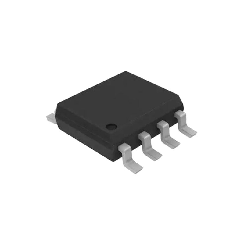
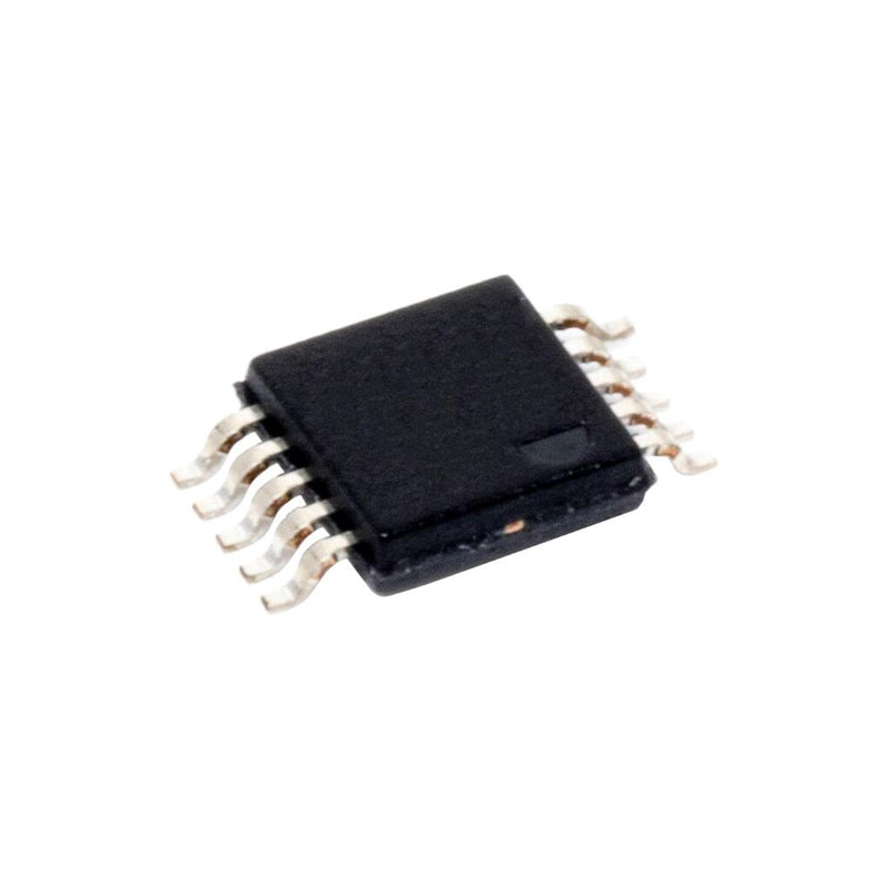
The AD8418 offers breakthrough performance throughout the −40°C to +125°C temperature range. It features a zero drift core, which leads to a typical offset drift of 0.1 µV/°C throughout the operating temperature range and the common-mode voltage range. The AD8418 is fully qualified for automotive applications and includes EMI filters and patented circuitry to enable output accuracy with pulse-width modulation (PWM) type input common-mode voltages. The typical input offset voltage is ±200 µV. The AD8418 is offered in 8-lead MSOP and SOIC packages.
ARBEITSTHEORIE
The AD8418 is a single-supply, zero drift, difference amplifier that uses a unique architecture to accurately amplify small differential current shunt voltages in the presence of rapidly changing common-mode voltages.
In typical applications, the AD8418 is used to measure current by amplifying the voltage across a shunt resistor connected to its inputs by a gain of 20 V/V . The AD8418 is designed to provide excellent common-mode rejection, even with PWM common-mode inputs that can change at very fast rates, for example, 1 V/ns. The AD8418 contains patented technology to eliminate the negative effects of such fast changing external common-mode variations.
The AD8418 features an input offset drift of less than 500 nV/°C. This performance is achieved through a novel zero drift architecture that does not compromise bandwidth, which is typically rated at 250 kHz.
The reference inputs, VREF1 and VREF2, are tied through 100 kΩresistors to the positive input of the main amplifier, which allows the output offset to be adjusted anywhere in the output operating range. The gain is 1 V/V from the reference pins to the output when the reference pins are used in parallel. When the pins are used to divide the supply, the gain is 0.5 V/V.
The AD8418 offers breakthrough performance without compromising any of the robust application needs typical of solenoid or motor control. The ability to reject PWM input common-mode voltages and the zero drift architecture providing low offset and offset drift allows the AD8418 to deliver total accuracy for these demanding applications.
UNIDIRECTIONAL OPERATION
Unidirectional operation allows the AD8418 to measure currents through a resistive shunt in one direction. The basic modes for unidirectional operation are ground referenced output mode and VS referenced output mode.
For unidirectional operation, the output can be set at the negative rail (near ground) or at the positive rail (near VS) when the differential input is 0 V. The output moves to the opposite rail when a correct polarity differential input voltage is applied. The required polarity of the differential input depends on the output voltage setting. If the output is set at the positive rail, the input polarity needs to be negative to move the output down. If the output is set at ground, the polarity must be positive to move the output up.
Ground Referenced Output
When using the AD8418 in this mode, both referenced inputs are tied to ground, which causes the output to sit at the negative rail when there are zero differential volts at the input.
BIDIRECTIONAL OPERATION
Bidirectional operation allows the AD8418 to measure currents through a resistive shunt in two directions.
In this case, the output is set anywhere within the output range. Typically, it is set at half-scale for equal range in both directions. In some cases, however, it is set at a voltage other than half scale when the bidirectional current is nonsymmetrical.
Adjusting the output is accomplished by applying voltage(s) to the referenced inputs.
VREF1 and VREF2 are tied to internal resistors that connect to an internal offset node. There is no operational difference between the pins.

