ALLGEMEINE BESCHREIBUNG
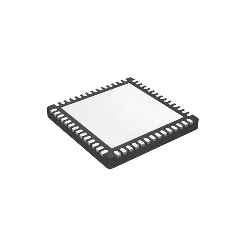
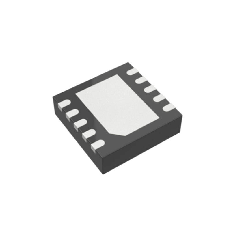
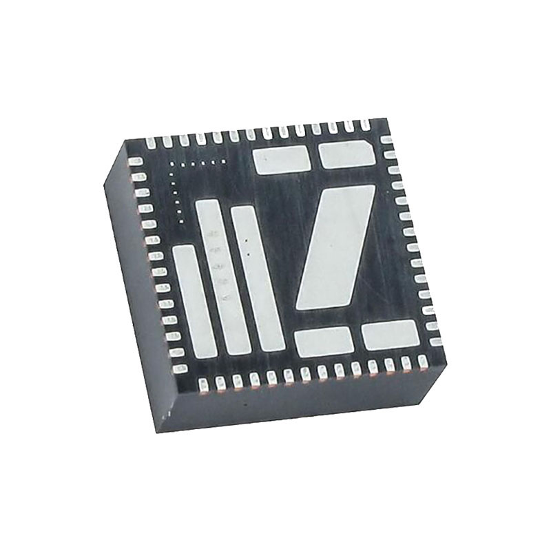
The AD9152 is a dual, 16-bit, high dynamic range digital-toanalog converter (DAC) that provides a maximum sample rate of 2.25 GSPS, permitting a multicarrier generation up to the Nyquist frequency. The DAC outputs are optimized to interface seamlessly with the ADRF6720 analog quadrature modulator (AQM) from Analog Devices, Inc. An optional 3-wire or 4-wire serial port interface (SPI) provides for programming/readback of many internal parameters. The full-scale output current can be programmed over a range of 4 mA to 20 mA. The AD9152 is available in a 56-lead LFCSP. The AD9152 is a member of the TxDAC+ family.
PRODUKT-HIGHLIGHTS
1.Ultrawide signal bandwidth enables emerging wideband and multiband wireless applications.
2.Advanced low spurious and distortion design techniques provide high quality synthesis of wideband signals from baseband to high intermediate frequencies.
3.JESD204B Subclass 1 support simplifies multichip synchronization in software and hardware design.
4.Fewer pins for data interface width with the serializer/ deserializer (SERDES) JESD204B four-lane interface.
5.Programmable transmit enable function allows easy design balance between power consumption and wake-up time.
6.Small package size with an 8 mm × 8 mm footprint.
FEATURES
Supports input data rates up to 1.125 GSPS
Proprietary low spurious and distortion design
Einzelträger LTE 20 MHz Bandbreite (BW), ACLR = 77 dBc bei 180 MHz IF
SFDR = 72 dBc at 150 MHz IF, −6 dBFS
Flexible 4-lane JESD204B interface
Synchronisierung mehrerer Chips
Feste Latenzzeit
Data generator latency compensation Selectable 1×, 2×, 4×, and 8× interpolation filter
Low power architecture Input signal power detection
Emergency stop for downstream analog circuitry protection
Transmit enable function allows extra power saving
High performance, low noise, phase-locked loop (PLL) clock multiplier
Digital inverse sinc filter and programmable finite impulse response (FIR) filter
Low power: 1223 mW at 1.5 GSPS, 1406 mW at 2.0 GSPS, full operating conditions
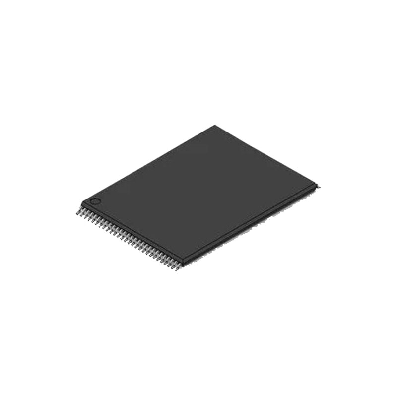
56-lead LFCSP with exposed pad
ANWENDUNGEN
Wireless communications
LTE- und GSM-Basisstationen mit mehreren Trägern
Breitband-Repeater
Softwaredefinierte Funkgeräte
Breitbandkommunikation
Point to point microwave radios
LMDS/MMDS
Transmit diversity, multiple input/multiple output (MIMO) Instrumentation
Automatisierte Testgeräte
ARBEITSTHEORIE
The AD9152 is a 16-bit, dual DAC with a SERDES interface. Four high speed serial lanes carry data at a maximum speed of 12.38 Gbps, and a 1.238 GSPS input data rate to the DACs. Compared to either LVDS or CMOS interfaces, the SERDES interface simplifies pin count, board layout, and input clock requirements to the device. The clock for the input data is derived from the device clock (required by the JESD204B specification). This device clock can be sourced with a PLL reference clock used by the on-chip PLL to generate a DAC clock, a high fidelity direct external DAC sampling clock, or a 2× DAC frequency RF clock. The device can be configured to operate in one-, two-, or four-lane modes, depending on the required input data rate. The digital datapath of the AD9152 offers four interpolation modes (1×, 2×, 4×, and 8×) through three half-band filters with a maximum DAC sample rate of 2.25 GSPS. An inverse sinc filter compensates for sinc related roll-off. The PFIR filter compensates the gain over frequency in a more flexible way. The AD9152 DAC cores provide a fully differential current output with a nominal full-scale current of 20 mA. The full-scale current, IOUTFS, is user adjustable to between 4.04 mA and 20.22 mA, typically. The differential current outputs are complementary and are optimized for easy integration with the Analog Devices ADRF6720 AQM. The AD9152 is capable of multichip synchronization that can both synchronize multiple DACs and establish a constant and deterministic latency (latency locking) path for the DACs. The latency for each of the DACs remains constant from link establishment to link establishment. An external alignment (SYSREF±) signal makes the AD9152 Subclass 1 compliant. Several modes of SYSREF± signal handling are available for use in the system. An SPI configures the various functional blocks and monitors their statuses. The various functional blocks and the data interface must be set up in a specific sequence for proper operation (see the Device Setup Guide section). Simple SPI initialization routines set up the JESD204B link and are included in the evaluation board package. The following sections describe the various blocks of the AD9152 in greater detail. Descriptions of the JESD204B interface, control parameters, and various registers to set up and monitor the device are provided. The recommended start-up routine reliably sets up the data link.

