ALLGEMEINE BESCHREIBUNG
The AD9216 is a dual, 3 V, 10-bit, 105 MSPS analog-to-digital converter (ADC). It features dual high performance sampleand-hold amplifiers (SHAs) and an integrated voltage reference. The AD9216 uses a multistage differential pipelined architecture with output error correction logic to provide 10-bit accuracy and guarantee no missing codes over the full operating temperature range at up to 105 MSPS data rates. The wide bandwidth, differential SHA allows for a variety of user selectable input ranges and offsets, including single-ended applications. The AD9216 is suitable for various applications, including multiplexed systems that switch full-scale voltage levels in successive channels and for sampling inputs at frequencies well beyond the Nyquist rate.
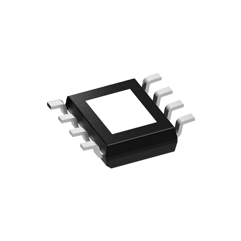
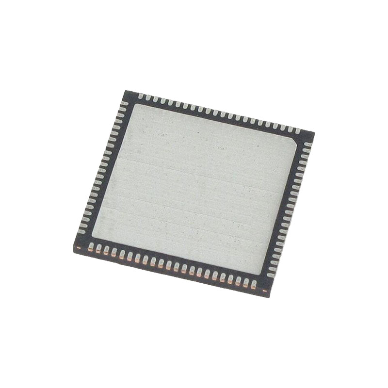
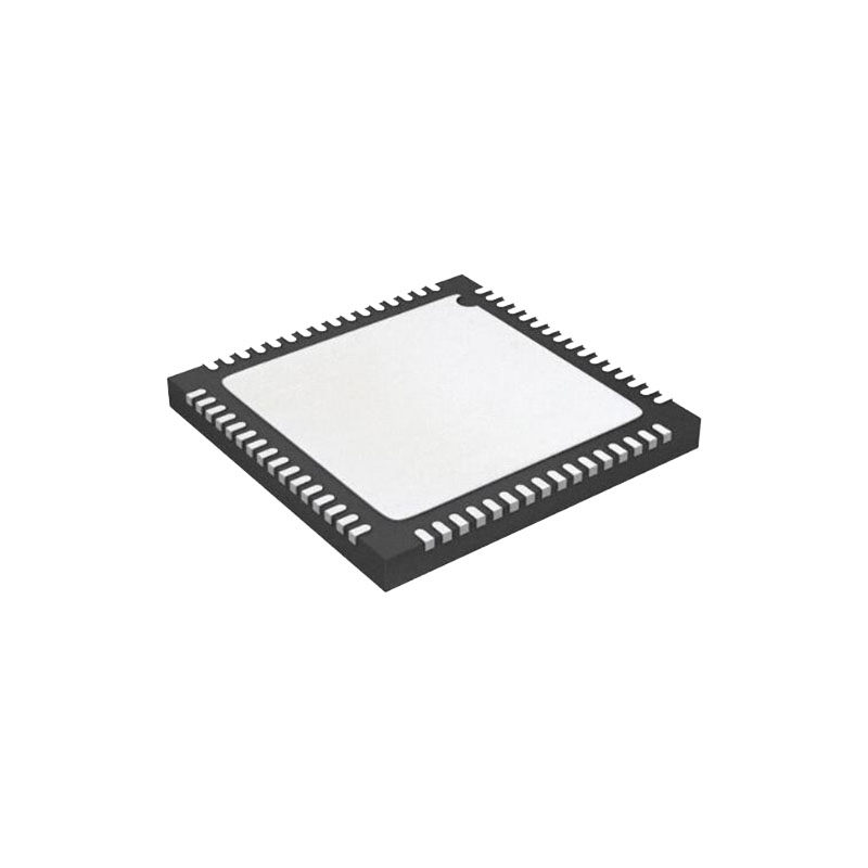
Dual single-ended clock inputs are used to control all internal conversion cycles. A duty cycle stabilizer is available on the AD9216 and can compensate for wide variations in the clock duty cycle, allowing the converters to maintain excellent performance. The digital output data is presented in either straight binary or twos complement format. Fabricated on an advanced CMOS process, the AD9216 is available in a space saving, Pb-free, 64-lead LFCSP (9 mm × 9 mm) and is specified over the industrial temperature range (−40°C to +85°C).
FEATURES
Integrated dual 10-bit ADC
Single 3 V supply operation
SNR = 57.6 dBc (to Nyquist, AD9216-105)
SFDR = 74 dBc (to Nyquist, AD9216-105)
Low power: 150 mW/ch at 105 MSPS
Differential input with 300 MHz 3 dB bandwidth
Exceptional crosstalk immunity < -80 dB
Offset Binär- oder Zweierkomplement-Datenformat
Taktstabilisator
ANWENDUNGEN
Ultraschallgeräte
IF sampling in communications receivers 3G, radio point-to-point, LMDS, MMDS
Batteriebetriebene Instrumente
Handgehaltene Skopemeter
Günstige digitale Oszilloskope
PRODUKT-HIGHLIGHTS
- Pin compatible with AD9238, dual 12-bit 20 MSPS/40 MSPS/ 65 MSPS ADCand AD9248, dual 14-bit 20 MSPS/40 MSPS/ 65 MSPS ADC.
- 105 MSPS capability allows for demanding, high frequency applications.
- Low power consumption: AD9216–105: 105 MSPS = 300 mW.
- The patented SHA input maintains excellent performance for input frequencies up to 200 MHz and can be configured for single-ended or differential operation.
- Typical channel crosstalk of < −80 dB at fIN up to 70 MHz.
- The clock duty cycle stabilizer maintains performance over a wide range of clock duty cycles.
ARBEITSTHEORIE
The AD9216 consists of two high performance ADCs that are based on the AD9215 converter core. The dual ADC paths are independent, except for a shared internal band gap reference source, VREF. Each of the ADC paths consists of a proprietary front end SHA followed by a pipelined, switched-capacitor ADC. The pipelined ADC is divided into three sections, consisting of a sample-and-hold amplifier, followed by seven 1.5-bit stages, and a final 3-bit flash. Each stage provides sufficient overlap to correct for flash errors in the preceding stages. The quantized outputs from each stage are combined through the digital correction logic block into a final 10-bit result. The pipelined architecture permits the first stage to operate on a new input sample, while the remaining stages operate on preceding samples. Sampling occurs on the rising edge of the respec tive clock.
Each stage of the pipeline, excluding the last, consists of a low resolution flash ADC and a residual multiplier to drive the next stage of the pipeline. The residual multiplier uses the flash ADC output to control a switched capacitor digital-to-analog converter (DAC) of the same resolution. The DAC output is subtracted from the stage’s input signal and the residual is amplified (multiplied) to drive the next pipeline stage. The residual multiplier stage is also called a multiplying DAC (MDAC). One bit of redundancy is used in each one of the stages to facilitate digital correction of flash errors. The last stage simply consists of a flash ADC.
The input stage contains a differential SHA that can be config ured as ac- or dc-coupled in differential or single-ended modes. The output-staging block aligns the data, carries out the error correction, and passes the data to the output buffers. The output buffers are powered from a separate supply, allowing adjustment of the output voltage swing.