ALLGEMEINE BESCHREIBUNG
The AD9513 features a three-output clock distribution IC in a design that emphasizes low jitter and phase noise to maximize data converter performance. Other applications with demanding phase noise and jitter requirements also benefit from this part.
There are three independent clock outputs that can be set to either LVDS or CMOS levels. These outputs operate to 800 MHz in LVDS mode and to 250 MHz in CMOS mode.
Each output has a programmable divider that can be set to divide by a selected set of integers ranging from 1 to 32. The phase of one clock output relative to the other clock output can be set by means of a divider phase select function that serves as a coarse timing adjustment.
One of the outputs features a delay element with three selectable full-scale delay values (1.8 ns, 6.0 ns, and 11.6 ns), each with 16 steps of fine adjustment.
The AD9513 does not require an external controller for operation or setup. The device is programmed by means of 11 pins (S0 to S10) using 4-level logic. The programming pins are internally biased to ⅓ VS. The VREF pin provides a level of ⅔ VS. VS (3.3 V) and GND (0 V) provide the other two logic levels.
The AD9513 is ideally suited for data converter clocking applications where maximum converter performance is achieved by encode signals with subpicosecond jitter.
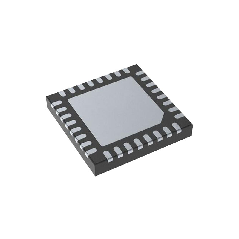
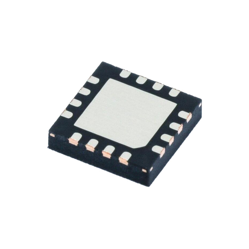
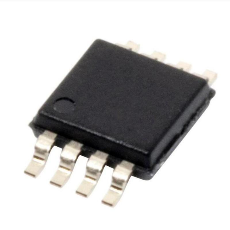
The AD9513 is available in a 32-lead LFCSP and operates from a single 3.3 V supply. The temperature range is −40°C to +85°C.
FEATURES
1.6 GHz differential clock input
3 programmable dividers
Divide-by in range from1 to 32
Phase select for coarse delay adjust
Three 800 MHz/250 MHz LVDS/CMOS clock outputs
Additive output jitter 300 fs rms
Time delays up to 11.6 ns
Device configured with 4-level logic pins
Space-saving, 32-lead LFCSP
ANWENDUNGEN
Low jitter, low phase noise clock distribution
Clocking high speed ADCs, DACs, DDSs, DDCs, DUCs, MxFEs High performance wireless transceivers
High performance instrumentation
Broadband infrastructure
ATE
TERMINOLOGIE
Phase Jitter and Phase Noise
An ideal sine wave can be thought of as having a continuous and even progression of phase with time from 0 to 360 degrees for each cycle. Actual signals, however, display a certain amount of variation from ideal phase progression over time. This phenomenon is called phase jitter. Although there are many causes that can contribute to phase jitter, one major component is due to random noise that is characterized statistically as being Gaussian (normal) in distribution.
This phase jitter leads to a spreading out of the energy of the sine wave in the frequency domain, producing a continuous power spectrum. This power spectrum is usually reported as a series of values whose units are dBc/Hz at a given offset in frequency from the sine wave (carrier). The value is a ratio (expressed in dB) of the power contained within a 1 Hz bandwidth with respect to the power at the carrier frequency. For each measurement, the offset from the carrier frequency is also given.
It is also meaningful to integrate the total power contained within some interval of offset frequencies (for example, 10 kHz to 10 MHz). This is called the integrated phase noise over that frequency offset interval and can be readily related to the time jitter due to the phase noise within that offset frequency interval.
Phase noise has a detrimental effect on the performance of ADCs, DACs, and RF mixers. It lowers the achievable dynamic range of the converters and mixers, although they are affected in somewhat different ways.
Time Jitter
Phase noise is a frequency domain phenomenon. In the time domain, the same effect is exhibited as time jitter. When observing a sine wave, the time of successive zero crossings is seen to vary. For a square wave, the time jitter is seen as a displacement of the edges from their ideal (regular) times of occurrence. In both cases, the variations in timing from the ideal are the time jitter. Since these variations are random in nature, the time jitter is specified in units of seconds root mean square (rms) or 1 sigma of the Gaussian distribution.
Time jitter that occurs on a sampling clock for a DAC or an ADC decreases the SNR and dynamic range of the converter. A sampling clock with the lowest possible jitter provides the highest performance from a given converter.
Additive Phase Noise
It is the amount of phase noise that is attributable to the device or subsystem being measured. The phase noise of any external oscillators or clock sources has been subtracted. This makes it possible to predict the degree to which the device as the total system phase noise when used in conjunction with the various oscillators and clock sources, each of which contribute their own phase noise to the total. In many cases, the phase noise of one element dominates the system phase noise.
Additive Time Jitter
It is the amount of time jitter that is attributable to the device or subsystem being measured. The time jitter of any external oscillators or clock sources has been subtracted. This makes it possible to predict the degree to which the device will affect the total system time jitter when used in conjunction with the various oscillators and clock sources, each of which contribute their own time jitter to the total. In many cases, the time jitter of the external oscillators and clock sources dominates the system time jitter.

