ALLGEMEINE BESCHREIBUNG
The ADA4800 is voltage buffer integrated with an active load. The buffer is a low power, high speed, low noise, high slew rate, fast settling, fixed gain of 1 monolithic amplifier for chargecoupled device (CCD) applications. For CCD applications, the active load current source (IAL) can load the open source CCD sensor outputs and the buffer can drive the AFE load. The active current load can also be switched off, to use the ADA4800 as just a unity gain buffer. The buffer consumes only 20 mW of static power. In applications where power savings is critical, the ADA4800 features a power save mode (see the Power Save Mode section), which further reduces the total current consumption. The bandwidth of the ADA4800 buffer is also fully adjustable through the IDRV pin.
The buffer of the ADA4800 employs a push-pull output stage architecture, providing drive current and maximum slew capability for both rising and falling signal transitions. At a 5 mA quiescent current setting, it provides 400 MHz, −3 dB bandwidth, which makes this buffer well suited for CCD sensors from machine vision to digital still camera applications.
The ADA4800 is ideal for driving the input of the Analog Devices, Inc., 12-bit and 14-bit high resolution analog front ends (AFE) such as the AD9928, AD9990, AD9920A, AD9923A, and AD997x family.
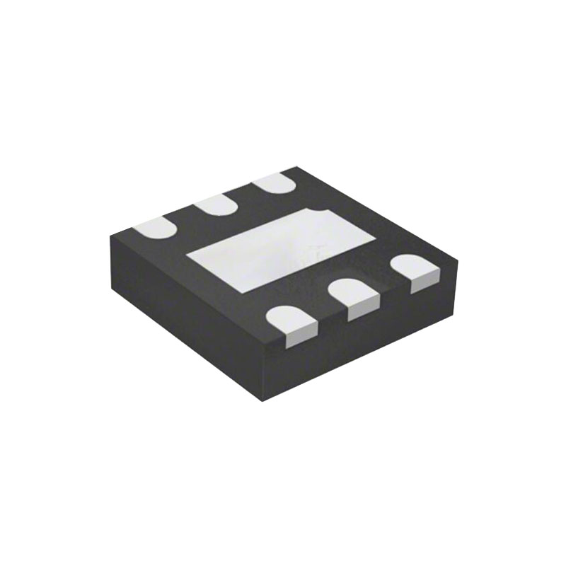
The versatility of the ADA4800 allows for seamless interfacing with many CCD sensors from various manufacturers. The ADA4800 is designed to operate at supply voltages as low as 4 V and up to 17 V. It is available in a 1.6 mm × 1.6 mm × 0.55 mm, 6-lead LFCSP package and is rated to operate over the industrial temperature range of −40℃ to +85℃.
FEATURES
Integrated active load and gain of 1 buffer
Very low buffer power consumption
As low as 20 mW on chip
Power save feature to reduce active load current by GPO
control
High buffer speed
400 MHz, −3 dB bandwidth
415 V/μs slew rate
Fast settling time to 1%, 2 V step: 5 ns
Adjustable buffer bandwidth
Push-pull output stage
Adjustable active load current
Small package: 1.6 mm × 1.6 mm × 0.55 mm
ANWENDUNGEN
CCD image sensor output buffer
Digital still cameras
Camcorders
POWER SUPPLY BYPASSING
Attention must be paid to bypassing the power supply pin of the ADA4800. Use high quality capacitors with low equivalent series resistance (ESR), such as multilayer ceramic capacitors (MLCCs), to minimize supply voltage ripple and power dissipation. A large, usually tantalum, 2.2 μF to 47 μF capacitor located in close proximity to the ADA4800 is required to provide good decoupling for lower frequency signals. The actual value is determined by the circuit transient and frequency requirements. In addition, 0.1 μF MLCC decoupling capacitors should be located as close to the power supply pin as is physically possible, no more than ⅛ inch away. The ground returns should terminate immediately into the ground plane. Locating the bypass capacitor return close to the load return minimizes ground loops and improves performance.
POWER SAVE MODE
The buffer of the ADA4800 consumes only 20 mW of static power. To achieve even more power savings, the ADA4800 active load current can be switched off during standby mode or reduced during monitoring mode.Power save mode allows IAL current to be logically controlled by connecting the ISF pin to any generalpurpose output (GPO) pin of the system microcontroller through an external resistor. A GPO logic high enables the flow of input sink current, while a logic low disables the input sink current and asserts the power save mode.
POWER SEQUENCING
With the ADA4800 supply turned off (VCC = 0 V), a voltage on an I/O pin can turn on the protection diodes and cause permanent damage or destroy the IC. To prevent this condition during power-on, no voltages should be applied to any I/O pins until VCC is fully on and settled. During power-off, I/O pin voltages should be removed or reduced to 0 V before VCC is turned off.

