FEATURES
Conversion loss: 7.5 dB typical at 5.5 GHz to 10 GHz
Local oscillator (LO) to radio frequency (RF) isolation: 45 dB
typical at 5.5 GHz to 10 GHz
LO to intermediate frequency (IF) isolation: 45 dB typical at
10 GHz to 14 GHz
Input third-order intercept (IIP3): 21 dBm typical at 10 GHz
to 14 GHz
Input P1dB: 11.5 dBm typical at 10 GHz to 14 GHz
Input second-order intercept (IIP2): 55 dBm typical at 10 GHz
to 14 GHz
Passive double-balanced topology
Wide IF bandwidth: dc to 6 GHz
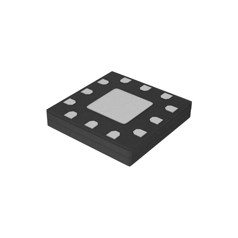
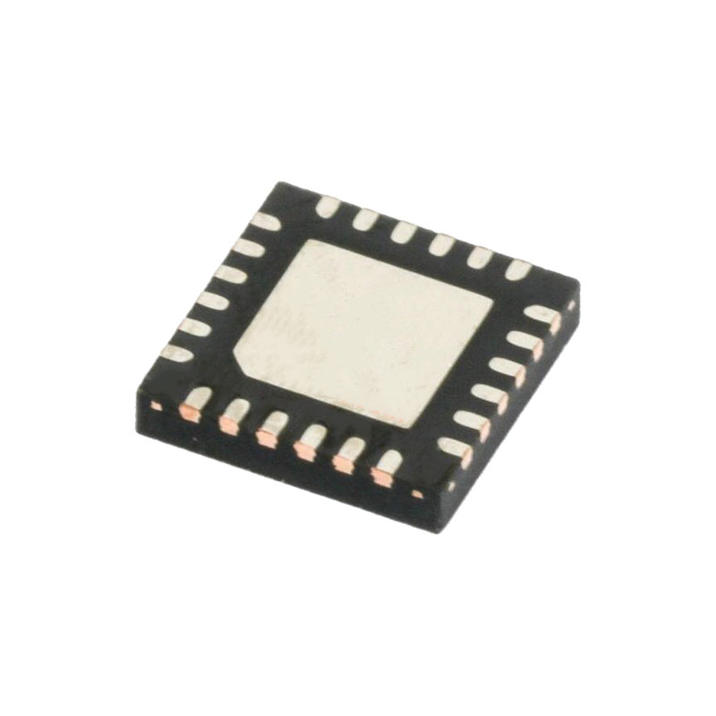
12-lead ceramic leadless chip carrier package
ANWENDUNGEN
Point to point microwave radios
Point to multipoint radios
Military end use
Instrumentation, automatic test equipment (ATE), and sensors
ALLGEMEINE BESCHREIBUNG
The HMC558A is a general-purpose, double-balanced mixer in a leadless RoHS compliant SMT package that can be used as an upconverter or downconverter between 5.5 GHz and 14 GHz. This mixer is fabricated in a gallium arsenide (GaAs) metal semi conductor field effect transistor (MESFET) process, and requires no external components or matching circuitry.
The HMC558A provides excellent LO to RF and LO to IF isolation due to optimized balun structures, and operates with LO drive levels as low as 9 dBm. The RoHS compliant HMC558A eliminates the need for wire bonding, and is compatible with high volume surface-mount manufacturing techniques.
ARBEITSTHEORIE
The HMC558A is a general-purpose double balanced mixer in a leadless RoHS compliant SMT package that can be used as an upconverter or downconverter between 5.5 GHz and 14 GHz. This mixer is fabricated in a GaAs MESFET process, and requires no external components or matching circuitry. The HMC558A provides excellent LO to RF and LO to IF isolation due to optimized balun structures and operates with LO drive levels as low as 9 dBm. The RoHS compliant HMC558A eliminates the need for wire bonding, and is compatible with high volume surface mount manufacturing techniques.
EVALUATION BOARD INFORMATION
The circuit board used in an application must use RF circuit design techniques. Signal lines must have 50 Ω impedance, and the package ground leads and exposed pad must be connected directly to the ground plane. Use a sufficient number of via holes to connect the top and bottom ground planes. The evaluation circuit board shown in Figure 35 is available from Analog Devices, Inc., upon request.

