Beschreibung
The LTC3603 is a high efficiency, monolithic synchronous step-down DC/DC converter utilizing a constant-frequency, current mode architecture. It operates from an input voltage range of 4.5V to 15V and provides an adjustable regulated output voltage from 0.6V to 14.5V while delivering up to 2.5A of output current. The internal synchronous power switch with 45mΩ on-resistance increases efficiency and eliminates the need for an external Schottky diode. The switching frequency can either be set by an external resistor or synchronized to an external clock. OPTI-LOOP compensation allows the transient response to be optimized over a wide range of loads and output capacitors.
The LTC3603 can be configured for either Burst Mode operation or forced continuous operation. Forced continuous operation reduces noise and RF interference, while Burst Mode operation provides the highest efficiency at light loads. In Burst Mode operation, external control of the burst clamp level allows the output voltage ripple to be adjusted according to the requirements of the application.
Eigenschaften
Wide Input Voltage Range: 4.5V to 15V
2.5A Output Current
Low RDS(ON) Internal Switches: 45mΩ and 85mΩ
Programmable Frequency: 300kHz to 3MHz
Low Quiescent Current: 75µA
0.6V ±1% Reference Allows Precise, Low Output Voltage
99% Maximum Duty Cycle
Adjustable Burst Mode® Clamp
Synchronisierbar mit externer Uhr
Power Good Output Voltage Monitor
Overtemperature Protection
Overvoltage Protection
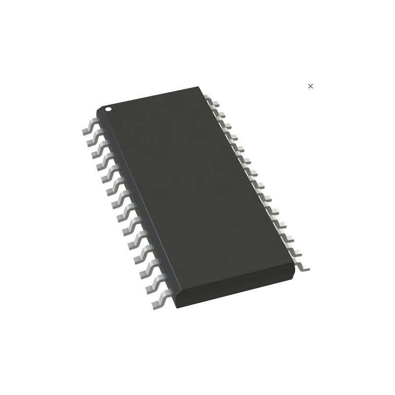
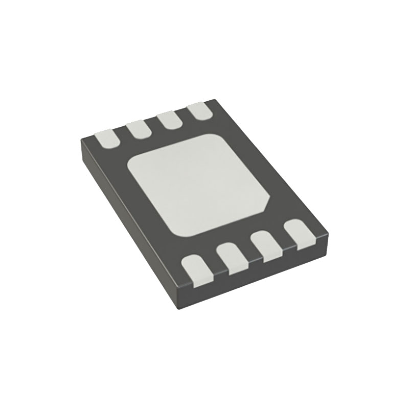
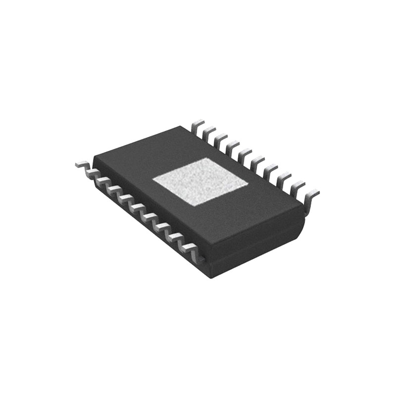
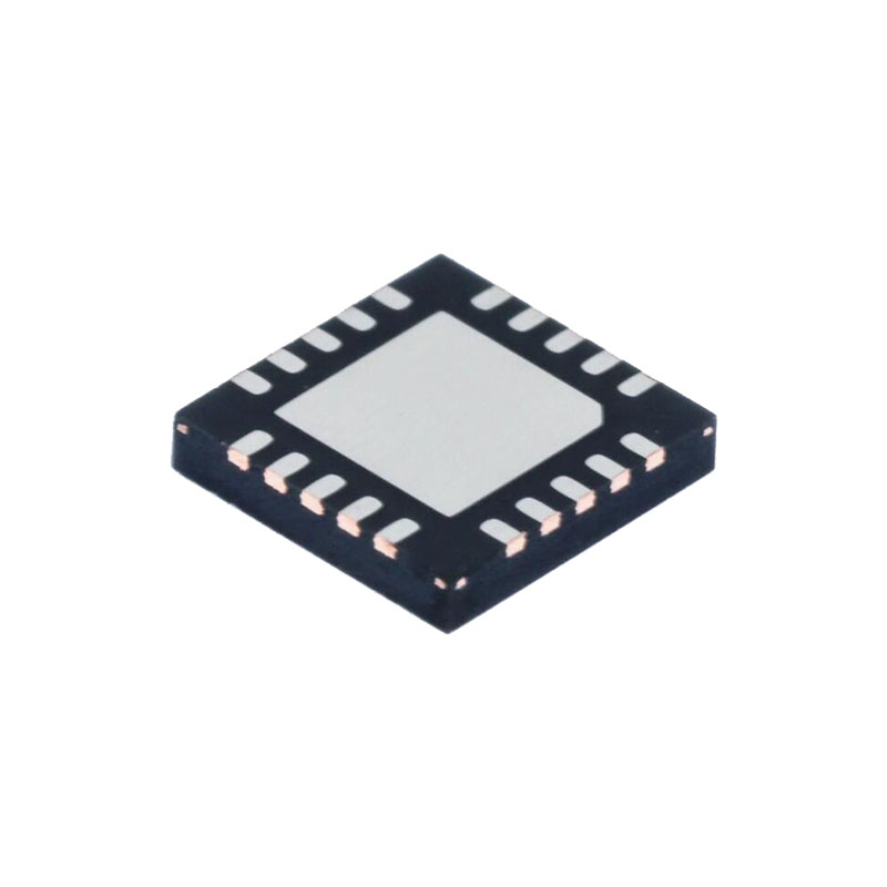
Available in 16-Lead Thermally Enhanced eMSOP and 4mm × 4mm QFN Packages
applications
Verbrauchsmaterial für die Ladestation
Portable Instruments
Communications Infrastructure
operation
Hauptkontrollschleife
The LTC3603 is a monolithic, constant-frequency, current mode step-down DC/DC converter. During normal operation, the internal top power switch (N-channel MOSFET) is turned on at the beginning of each clock cycle. Current in the inductor increases until the current comparator trips and turns off the top power MOSFET. The peak inductor current at which the current comparator shuts off the top power switch is controlled by the voltage on the ITH pin. The error amplifier adjusts the voltage on the ITH pin by comparing the feedback signal from a resistor divider on the VFB pin with an internal 0.6V reference. When the load current increases, it causes a reduction in the feedback voltage relative to the reference. The error amplifier raises the ITH voltage until the average inductor current matches the new load current. When the top power MOSFET shuts off, the synchronous power switch (N-channel MOSFET) turns on until either the bottom current limit is reached or the beginning of the next clock cycle. The bottom current limit is set at –2.5A for forced continuous mode and 0A for Burst Mode operation.
Forced Continuous Mode
Connecting the SYNC/MODE pin to INTVCC will disable Burst Mode operation and forced continuous current operation. At light loads, forced continuous mode operation is less efficient than Burst Mode operation, but may be desirable in some applications where it is necessary to keep switching harmonics out of a signal band. The output voltage ripple is minimized in this mode.
Betrieb im Burst-Modus
Connecting the SYNC/MODE pin to a voltage in the range of 0.42V to 1V enables Burst Mode operation. In Burst Mode operation, the internal power MOSFETs operate intermittently at light loads. This increases efficiency by minimizing switching losses. During Burst Mode operation, the minimum peak inductor current is externally set by the voltage on the SYNC/MODE pin and the voltage on the ITH pin is monitored by the burst comparator to determine when sleep mode is enabled and disabled. When the average inductor current is greater than the load current, the voltage on the ITH pin drops. As the ITH voltage falls below 330mV, the burst comparator trips and enables sleep mode. During sleep mode, the top power MOSFET is held off and the ITH pin is disconnected from the output of the error amplifier. The majority of the internal circuitry is also turned off to reduce the quiescent current to 75µA while the load current is solely supplied by the output capacitor. When the output voltage drops, the ITH pin is reconnected to the output of the error amplifier and the top power MOSFET along with all the internal circuitry is switched back on. This process repeats at a rate that is dependent on the load demand. Pulse-skipping operation is implemented by connecting the SYNC/MODE pin to ground. This forces the burst clamp level to be at 0V. As the load current decreases, the peak inductor current will be determined by the voltage on the ITH pin until the ITH voltage drops below 330mV. At this point, the peak inductor current is determined by the minimum on-time of the current comparator. If the load demand is less than the average of the minimum on-time inductor current, switching cycles will be skipped to keep the output voltage in regulation.