Merkmale
6A Ausgangsstrom
2.25V bis 5.5V Eingangsspannungsbereich
Burst Mode® Betrieb mit niedriger Ausgangswelligkeit: IQ = 75µA
±1% Genauigkeit der Ausgangsspannung
Ausgangsspannung bis zu 0,6V
Hohe Effizienz: Bis zu 95%
Niedriger Dropout-Betrieb: 100% Einschaltdauer
Programmierbare Slew Rate am SW-Knoten reduziert Rauschen und EMI
Einstellbare Schaltfrequenz: Bis zu 4MHz
Optionale aktive Spannungspositionierung (AVP) mit interner Kompensation
Wählbarer Pulse-Skipping/Forced Continuous/Burst-Betrieb mit einstellbarer Burst-Klemme
Programmierbarer Soft-Start
Eingänge für Start-Up Tracking oder externe Referenz
DDR-Speicher-Modus, IOUT = ±3A
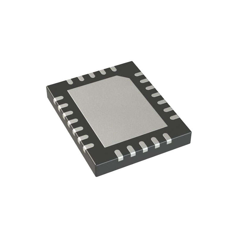
Erhältlich in einem 24-Pin 3mm × 5mm QFN Thermally Enhanced Gehäuse
anwendungen
Verbrauchsmaterial für die Ladestation
Verteilte Stromversorgungen
Tragbare Computer-Systeme
DDR-Speicher Terminierung
Handheld-Geräte
BeschreiBung
Der LTC®3616 ist ein monolithischer synchroner Abwärtsregler mit niedrigem Ruhestrom, der eine Current-Mode-Architektur mit konstanter Frequenz verwendet. Der Ruhestrom der DC-Versorgung im Sleep-Modus beträgt nur 70µA, während die Ausgangsspannung (Burst-Mode-Betrieb) bei Nulllast aufrechterhalten wird und beim Herunterfahren auf Null sinkt. Mit einem Eingangsspannungsbereich von 2,25V bis 5,5V eignet sich der LTC3616 ideal für Anwendungen mit einer einzelnen Li-Ion-Batterie sowie für Anwendungen mit fester niedriger Eingangsspannung. Die 100%-Tastverhältnis-Fähigkeit sorgt für einen niedrigen Dropout-Betrieb und verlängert so die Betriebszeit in batteriebetriebenen Systemen.
Die Betriebsfrequenz ist extern bis zu 4MHz programmierbar, was die Verwendung kleiner oberflächenmontierter Induktivitäten ermöglicht. Für rauschempfindliche Anwendungen kann der LTC3616 mit einem externen Taktgeber mit bis zu 4MHz synchronisiert werden.
Der erzwungene Dauermodusbetrieb des LTC3616 reduziert Rauschen und HF-Störungen. Dank der einstellbaren Kompensation kann das Einschwingverhalten über einen breiten Bereich von Lasten und Ausgangskondensatoren optimiert werden.
Der interne Synchronschalter erhöht den Wirkungsgrad und macht eine externe Catch-Diode überflüssig, wodurch externe Bauteile und Platinenplatz eingespart werden. Der LTC3616 wird in einem bleifreien, 3mm × 5mm großen, thermisch optimierten QFN-Gehäuse mit 24 Pins angeboten.
operaTion
Hauptkontrollschleife
Der LTC3616 ist ein monolithischer DC/DC-Abwärtswandler mit konstanter Frequenz und Strombetrieb. Im Normalbetrieb wird der interne obere Leistungsschalter (P-Kanal-MOSFET) zu Beginn jedes Taktzyklus eingeschaltet. Der Strom in der Induktivität steigt an, bis der Stromkomparator auslöst und den oberen Leistungsschalter ausschaltet. Der Spitzenstrom in der Induktivität, bei dem der Stromkomparator auslöst, wird durch die Spannung am ITH-Pin gesteuert. Der Fehlerverstärker stellt die Spannung am ITH-Pin ein, indem er das Rückkopplungssignal von einem Widerstandsteiler am VFB-Pin mit einer internen 0,6V-Referenz vergleicht. Wenn der Laststrom ansteigt, führt dies zu einer Verringerung der Rückkopplungsspannung im Verhältnis zur Referenz. Der Fehlerverstärker erhöht die ITH-Spannung, bis der durchschnittliche Induktorstrom mit dem neuen Laststrom übereinstimmt. Der typische Spannungsbereich für den ITH-Pin liegt zwischen 0,1V und 1,05V, wobei 0,45V dem Nullstrom entspricht.
Wenn sich der obere Leistungsschalter ausschaltet, schaltet sich der synchrone Leistungsschalter (N-Kanal MOSFET) ein, bis entweder die untere Stromgrenze erreicht ist oder der nächste Taktzyklus beginnt. Die untere Stromgrenze ist typischerweise auf -8A für den erzwungenen kontinuierlichen Modus und 0A für den Burst Mode Betrieb und den Pulse-Skipping Modus eingestellt.
Die Betriebsfrequenz ist standardmäßig auf 2,25MHz eingestellt, wenn RT/SYNC mit SVIN verbunden ist. Sie kann auch durch einen externen Widerstand zwischen dem RT/SYNC-Pin und Masse oder durch ein an den RT/SYNC-Pin angelegtes Taktsignal eingestellt werden. Die Schaltfrequenz kann zwischen 300kHz und 4MHz eingestellt werden.
Überspannungs- und Unterspannungskomparatoren ziehen den PGOOD-Ausgang auf Low, wenn die Ausgangsspannung um mehr als ±7,5% (typisch) vom Sollwert abweicht.
Burst-Modus-Betrieb - Interne Klammer
Wenn Sie den MODE-Pin mit SGND verbinden, wird der Burst Mode-Betrieb mit einer internen Klemme aktiviert. Im Burst-Mode-Betrieb arbeiten die internen Leistungsschalter bei geringer Last intermittierend. Dies erhöht den Wirkungsgrad durch Minimierung der Schaltverluste. Während der Intervalle, in denen die Schalter inaktiv sind, geht der LTC3616 in den Ruhezustand über, in dem viele der internen Schaltungen deaktiviert sind, um Strom zu sparen. Während des Burst-Modus-Betriebs wird der minimale Induktionsspitzenstrom intern geklemmt und die Spannung am ITH-Pin wird vom Burst-Komparator überwacht, um zu bestimmen, wann der Schlafmodus aktiviert und deaktiviert wird. Wenn der durchschnittliche Induktionsstrom größer ist als der Laststrom, fällt die Spannung am ITH-Pin. Wenn die ITH-Spannung unter die interne Klemme fällt, löst der Burstkomparator aus und aktiviert den Schlafmodus. Während des Ruhezustands werden die Leistungs-MOSFETs ausgeschaltet und der Laststrom wird ausschließlich vom Ausgangskondensator geliefert. Wenn die Ausgangsspannung abfällt, wird der obere Leistungsschalter wieder eingeschaltet und die internen Schaltungen werden wieder aktiviert. Dieser Vorgang wiederholt sich in einem Rhythmus, der vom Laststrom abhängig ist