BESCHREIBUNG
The LTC6560 is a low-noise, transimpedance amplifier (TIA) with 220MHz bandwidth. The LTC6560’s low noise, high transimpedance and low power dissipation are ideal for LIDAR receivers using avalanche photodiodes (APDs). The LTC6560 features 74kΩ transimpedance gain and 30µA linear input current range. Using an input circuit with a total input capacitance of 2pF, the input current noise density is 4.8pA/√Hz at 200MHz. With lower capacitance, noise and bandwidth improve further. The LTC6560 operates from a single 5V supply and consumes only 90mW. Utilizing the LTC6560’s output MUX, multiple LTC6560 devices can be combined to a single output. The LTC6560’s fast overload recovery and fast output MUXing make it well suited for LIDAR receivers with multiple APDs. Its single-ended output can swing 2VP-P on a 100Ω load. Its low impedance op amp style output has been designed to drive back-terminated 50Ω cables.
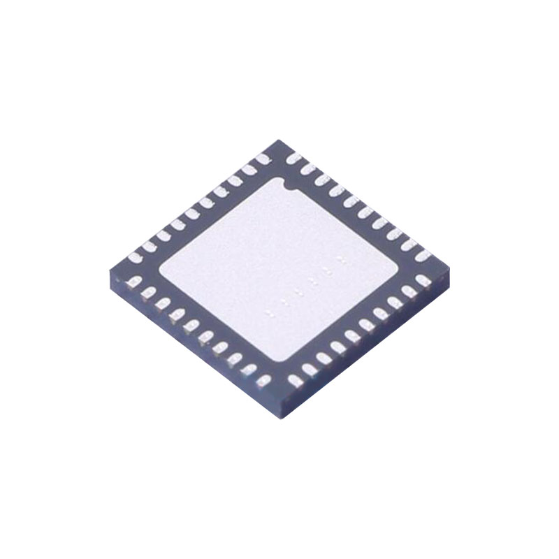
The LTC6560 is packaged in a compact 3mm × 3mm 16-pin leadless QFN package with an exposed pad for thermal management and low inductance.
FEATURES
220MHz –3dB Bandwidth with 2pF Input Capacitance
Single-Ended Output
74kΩ Transimpedance Gain
4.8pA/√Hz Input Current Noise Density at 200MHz (2pF)
64nARMS Integrated Input Current Noise Over 200MHz (2pF)
Linear Input Range 0µA to 30µA
Overload Current > ±400mA Peak
Fast Overload Recovery: 1mA in 10ns
Fast Output MUXing: <50ns
Einzelne 5V Versorgung
90mW Power Dissipation
2VP-P Output Swing on 100Ω Load
3mm × 3mm, 16-Lead QFN Package
Output MUX Combines Multiple LTC6560 Devices
AEC-Q100 qualifiziert für Automobilanwendungen
ANWENDUNGEN
LIDAR Receiver
Industrial Imaging
OPERATION
The LTC6560 is a transimpedance amplifier with output MUXing. A transimpedance amplifier converts an input current to an output voltage. The output multiplexer capability (O_MUX) allows multiple single channel LTC6560 devices to be combined. For example 2, 4, 6 or 8 current input channels are easily multiplexed into a single voltage output.
In typical LIDAR applications, the LTC6560 amplifies the output current of an APD. APDs are biased near breakdown to achieve high current gain. Under intense optical illumination they can conduct large currents, often in excess of 1A. The LTC6560 survives and quickly recovers from large overload currents of this magnitude. Rapid overload recovery is critical for LIDAR applications. During recovery, any TIA is blinded from subsequent pulses. The LTC6560 recovers from 1mA saturation events in less than 12ns without phase reversal, minimizing this form of data loss. As the level of input current exceeds the linear range, the output pulse width will widen. However, the recovery time remains in the 10’s of ns.
Internally the LTC6560 consists of multiple stages. The first stage is a transimpedance amplifier. A second voltage gain stage leads to a final output buffer that can drive a 2VP-P swing into a 100Ω load.
To increase a LIDAR system’s spatial resolution, many APDs are deployed, often in an array. To achieve maximum bandwidth, each APD pixel must have a dedicated TIA, as increasing CIN will reduce bandwidth. The LTC6560 output multiplexing capability allows compact multichannel designs without external multiplexers. The use of multiple LTC6560s works well with multiple single APDs to minimize trace capacitance, cost and solution size.
ANWENDUNGSINFORMATIONEN
External Bypassing
The LTC6560 has separate supply pins for input (VCCI) and output (VCCO), both of which should be bypassed with 1000pF and 0.1µF capacitors to ground. For simplest operation, the input and output supplies should be set to the same voltage.
The LTC6560 has a small internal bypass capacitor connected between the VREF pin and ground to ensure low input noise. For the lowest possible input noise, the VREF pin should also be bypassed externally with a high quality 0.1µF ceramic capacitor to ground. This bypass cap should be located physically close the VREF pin.