BESCHREIBUNG
The LTM4628 is a complete dual 8A output switching mode DC/DC power supply and can be easily configured to provide a single 2-phase 16A output. Included in the package are the switching controller, power FETs, inductor, and all supporting components. Operating from an input voltage range of 4.5V to 26.5V, the LTM4628 supports two outputs each with an output voltage range of 0.6V to 5.5V, set by a single external resistor. Its high efficiency design delivers 8A continuous current for each output. Only a few input and output capacitors are needed.
The device supports frequency synchronization, multiphase operation, Burst Mode operation and output voltage tracking for supply rail sequencing. It has an onboard temperature diode for device temperature monitoring. High switching frequency and a current mode architec
ture enable a very fast transient response to line and load changes without sacrificing stability.
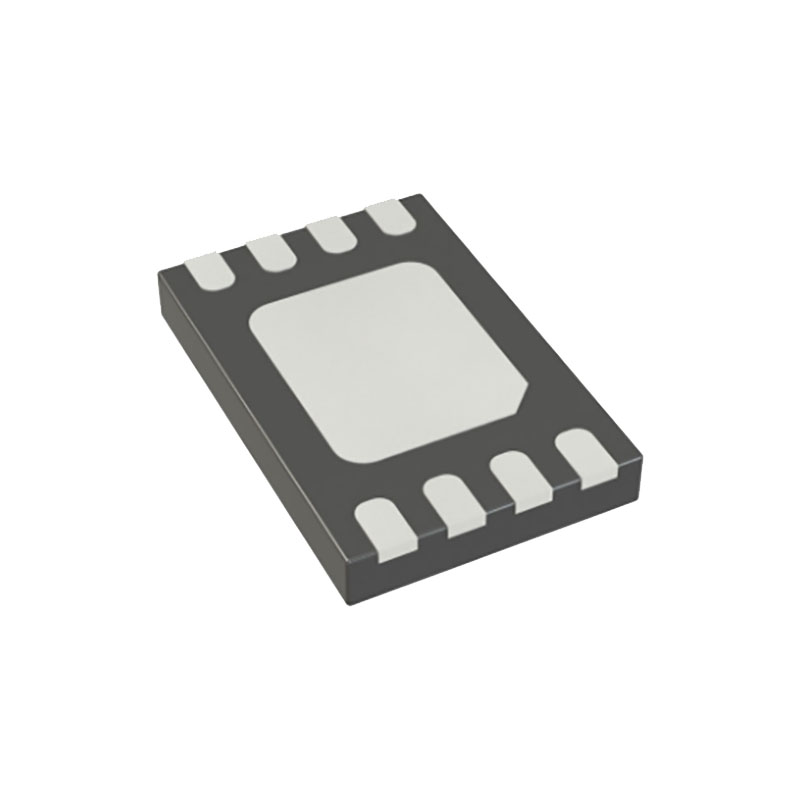
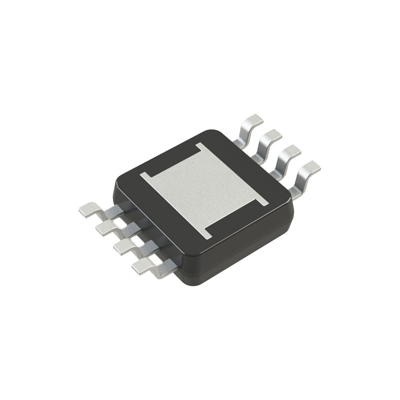
Fault protection features include overvoltage and overcurrent protection. The power module is offered in space saving and thermally enhanced 15mm × 15mm × 4.32mm LGA and 15mm × 15mm × 4.92mm BGA packages. The LTM4628 is available with SnPb (BGA) or RoHS-compliant terminal finish.
FEATURES
Complete Standalone Dual Power Supply
Single 16A or Dual 8A Output
Breiter Eingangsspannungsbereich: 4,5V bis 26,5V
Output Voltage Range: 0.6V to 5.5V
±1.5% Total DC Output Error
Differential-Fernerkennungsverstärker
Steuerung im Strommodus/schnelles Einschwingverhalten
Einstellbare Schaltfrequenz
Überstromschutz (Foldback)
Multiphase Parallel Current Sharing with Multiple LTM4628s
Frequenz-Synchronisation
Interne Temperatursensor-Diode Ausgang
Wählbarer Burst Mode® Betrieb
Soft-Start/Spannungsnachführung
Überspannungsschutz am Ausgang
Kleine Grundfläche für die Oberflächenmontage, niedriges Profil
15mm × 15mm × 4.32mm LGA and
15mm × 15mm × 4.92mm BGA Packages
ANWENDUNGEN
Telekommunikations- und Netzwerkausrüstung
Lagerung und ATCA-Karten
Industrielle Ausrüstung
ANWENDUNGSINFORMATIONEN
The typical LTM4628 application circuit is shown in Figure 28. External component selection is primarily determined by the maximum load current and output voltage. See Table 4 for specific external capacitor requirements for particular applications.VIN to VOUT Step-Down Ratios
There are restrictions in the maximum VIN and VOUT stepdown ratio that can be achieved for a given input voltage. Each output of the LTM4628 is capable of 98% duty cycle, but the VIN to VOUT minimum dropout is still shown as a function of its load current and will limit output current capability related to high duty cycle on the top side switch. Minimum on-time tON(MIN) is another consideration in operating at a specified duty cycle while operating at a certainfrequency due to the fact that tON(MIN) < D/fSW, where D is duty cycle and fSW is the switching frequency. tON(MIN) is specified in the electrical parameters as 90ns.
For parallel operation of multiple channels, the same feedback setting resistor can be used for the parallel design. This is done by connecting the VOUTS1 to the output as shown in Figure 2, thus tying one of the internal 60.4k resistors to the output. All of the VFB pins tie together with
one programming resistor as shown in Figure 2. In parallel operation, the VFB pins have an IFB current of 20nA maximum each channel. To reduce output voltage error due to this current, an additional VOUTS pin can be tied to VOUT, and an additional RFB resistor can be used to lower the total Thevenin’s equivalent resistance seen by this current. For example in Figure 2, the total
Thevenin’s equivalent resistance of the VFB pin is (60.4k // RFB), which is 30.2k where RFB is equal to 60.4k for a 1.2V output. Four phases connected in parallel equates to a worse case feedback current of 4•IFB equals 80nA maximum. The voltage error is 80nA•30.2k = 2.4mV. If
VOUTS2 is connected as shown in Figure 2 to VOUT, and another 60.4k resistor is connected from VFB2 to ground, then the voltage error is reduced to 1.2mV. If the voltage error is acceptable then no additional connections are necessary. The onboard 60.4k resistor is 0.5% accurate
and the VFB resistor can be chosen by the user to be as accurate as needed.
All COMP pins are tied together for current sharing between the phases. The TRACK pins can be tied together and a single soft-start capacitor can be used to softstart the regulator. The soft-start equation will need to have the soft-start current parameter increased by the number of paralleled channels. See the Output Voltage Tracking section.