BESCHREIBUNG
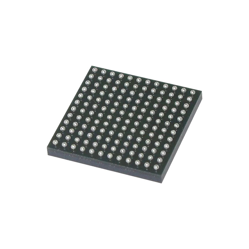
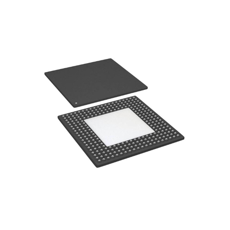
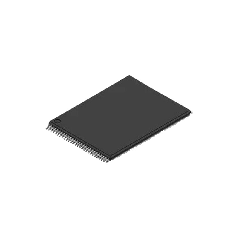
The LTM4630-1A/LTM4630-1B are dual 18A or single 36A output step-down μModule (power module) regulators with ±0.8% (LTM4630-1A) and ±1.5% (LTM4630-1B) total DC output error, respectively, which is very capable to achieve ±3% total output error including transients. Included in the package are the switching controller, power FETs, inductors, and all supporting components. External compensation allows for fast transient response to minimize output capacitance when powering FPGAs, ASICs, and processors. With synchronized multiphase parallel current sharing, four LTM4630-1 devices can deliver up to 144A. The LTM4630-1 is offered in a 16mm × 16mm × 5.01 BGA package.
FEATURES
±0.8% Maximum Total DC Output Error Over Line, Load, and Temperature (LTM4630-1A)
±3% Total Output Error, Including Transients with Minimum Output Capacitance
Dual 18A or Single 36A Output
4.5V to 15V Input, 0.6V to 1.8V Output Voltage Range
Differential-Fernerkennungsverstärker
Steuerung im Strommodus/schnelles Einschwingverhalten
Current Sharing Up to 144A
16mm × 16mm × 5,01mm BGA-Gehäuse
ANWENDUNGEN
FPGA, ASIC, μProcessor Core Voltage Regulation
Information, Communication Systems
OPERATION
Power Module Description
The LTM4630-1 is a dual-output standalone nonisolated switching mode DC/DC power supply with ±0.8% total DC output error over line, load, and temperature variation. It can provide two 18A outputs or single 36A output with few external input and output capacitors and setup components. This module provides precisely regulated output voltages programmable via external resistors from 0.6VDC to 1.8VDC over 4.5V to 15V input voltages.
The LTM4630-1 has dual integrated constant-frequency current mode regulators and built-in power MOSFET devices with fast switching speed. The typical switching frequency is 500kHz. For switching-noise sensitive applications, it can be externally synchronized from 400kHz to 750kHz. A resistor can be used to program a free run frequency on the fSET pin.
With current mode control, multi LTM4630-1s can be easily paralleled to provide up to 144A current with guaranteed perfect current sharing. Also, with current mode control, the LTM4630-1 module is able to achieve sufficient stability margins and a very fast ±3% output error including transients with a minimum number of output capacitors, even with all ceramic output capacitors.
This makes LTM4630-1 the best candidate when powering FPGAs, ASICs and processors in terms of DC accuracy, AC transient response, high output current, and accuracy current sharing.
Current mode control provides cycle-by-cycle fast current limit and foldback current limit in an overcurrent condition. Internal overvoltage and undervoltage comparators pull the open-drain PGOOD outputs low if the output feedback voltage exits a ±10% window around the regulation point. As the output voltage exceeds 10% above regulation, the bottom MOSFET will turn on to clamp the output voltage. The top MOSFET will be turned off. This overvoltage protect is feedback voltage referred.
Pulling the RUN pins below 1.1V forces the regulators into a shutdown state, by turning off both MOSFETs. The TRACK pins are used for programming the output voltage ramp and voltage tracking during start-up or used for soft-starting the regulator.
The LTM4630-1 has a built-in 10pF high frequency filter capacitor from COMP to SGND for each output. An external RC filtering circuit is required to achieve fast Type II control loop compensation. Table 4 provides a guide line for input, output capacitances, and RC COMP values for several operating conditions. The Analog Devices μModule power design tool (LTpowerCAD®) provides transient and stability analysis. The VFB pin is used to program the output voltage with a single external resistor to ground. A differential remote sense amplifier is available for sensing the output voltage accurately on one of the outputs at the load point, or in parallel operation sensing the output voltage at the load point.
High efficiency at light loads can be accomplished with selectable Burst Mode operation or pulse-skipping operation using the MODE_PLLIN pin. These light load features will accommodate battery operation. Efficiency graphs are provided for light load operation in the Typical Performance Characteristics section.
A general-purpose temperature diode is included inside the module to monitor the temperature of the module.
The switch pins are available for functional operation monitoring and a resistor-capacitor snubber circuit can be careful placed on the switch pin to ground to dampen any high frequency ringing on the transition edges.

