Allgemeine Beschreibung
The MAX3658 is a transimpedance preamplifier for receivers operating up to 622Mbps. Low noise, high gain, and low power dissipation make it ideal for fiber access and small form-factor transceivers.
The MAX3658 features 45nA input-referred noise, 18kΩ transimpedance gain, 580MHz bandwidth, and 2mAP-P input overload. Operating from a +3.3V supply, the MAX3658 consumes only 66mW. An integrated filter resistor provides positive bias for the photodiode. These features, combined with a small die size, allow easy assembly into a TO-46 header with a photodiode. The MAX3658 also includes an average photocurrent monitor.
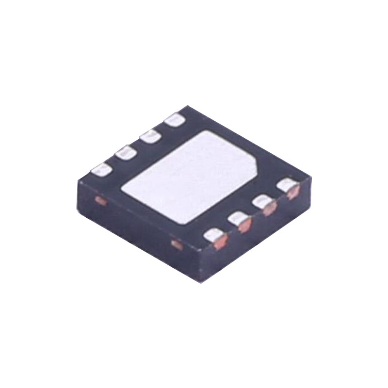
The MAX3658 has typical optical sensitivity of -33dBm (0.9A/W), which exceeds the class-B APON requirements. Typical optical overload is 1dBm. The MAX3658 is available in die form with both output polarities (MAX3658A and MAX3658B). The MAX3658A is also available in a 3mm x 3mm 8-pin TDFN package.
Anwendungen
Optical Receivers (Up to 622Mbps Operation)
Passive Optical Networks
SFF/SFP Transceivers
FTTx Transceivers
Eigenschaften
45nARMSNoise, -33dBm Sensitivity
18.3kΩTransimpedance Gain
580MHz Bandwidth
2mAP-PInput Overload, 1dBm Overload
66mW Power Dissipation
3.3V Operation
Average Photocurrent Monitor
Detaillierte Beschreibung
The MAX3658 transimpedance amplifier is designed for 622Mbps fiber optic applications. The MAX3658 is comprised of a transimpedance amplifier, a voltage amplifier, an output buffer, a DC cancellation circuit, and a photocurrent monitor.
Output Buffer
The output buffer is designed to drive a 150Ω differential load between OUT+ and OUT-. For optimum supply noise rejection, the MAX3658 should be terminated with a differential load. The MAX3658 single-ended outputs do not drive a DC-coupled grounded load. The outputs should be AC-coupled or terminated to VCC. If a singleended output is required, both the used and the unused outputs should be terminated in a similar manner.
DC Cancellation Circuit
The DC cancellation circuit uses low-frequency feedback to remove the DC component of the input signal. This feature centers the input signal within the transimpedance amplifier’s linear range, thereby reducing pulse-width distortion.
The DC cancellation circuit is internally compensated and does not require external capacitors. This circuit minimizes pulse-width distortion for data sequences that exhibit a 50% mark density. A mark density significantly different from 50% causes the MAX3658 to generate pulse-width distortion. Grounding the FILT pin disables the DC cancellation circuit. For normal operation, the DC cancellation circuit must be enabled.
The DC cancellation current is drawn from the input and creates noise. For low-level signals with little or no DC component, the added noise is insignificant. However, amplifier noise increases for signals with significant DC component.
Photocurrent Monitor
The MAX3658 includes an average photocurrent monitor. The current sourced from MON to ground is approximately equal to the DC current at IN.
Design Procedure
Select Photodiode
Noise performance and bandwidth are adversely affected by capacitance on the TIA input node. Select a lowcapacitance photodiode to minimize the total input capacitance on this pin. The MAX3658 is optimized for 0.5pF of capacitance on the input. Assembling the MAX3658 in die form using chip and wire technology provides the lowest capacitance input and the best possible performance.
Select Supply Filter
Sensitive optical receivers require wide-band powersupply decoupling. Power-supply bypassing should provide low impedance between VCC and ground for frequencies between 10kHz and 700MHz. Isolate the MAX3658 from noise sources with LC supply filters and shielding. Place a supply filter (CVCC2) as close to the MAX3658 as possible.
Select Output Filter
Input sensitivity is improved by adding a filter between TIA and the quantizer/limiting amplifier, with 0.5pF input capacitance. Typical bandwidth of the MAX3658 is 580MHz; the highest expected bandwidth is 730MHz.
Wire Bonding
For high-current density and reliable operation, the MAX3658 uses gold metalization. For best results, use gold-wire ball-bonding techniques. Use caution when wedge bonding. Die-size is 52 mils x 29 mils, (1.32mm x 0.736mm) and die thickness is 15 mils (380µm). The bond-pad passivation opening is 75µm and bond-pad metal thickness is 5µm.Understanding Bonding Coordinates and Physical Die Size for additional information on bondpad coordinates.

