General Description
The MAX40263 is a dual-channel operational amplifier with two channels that can be disabled separately with two individual pins.
The MAX40263 offers a unique combination of high speed, precision, and low-voltage operation, making it ideally suited for a large number of signal-processing functions such as filtering and amplification of signals in portable and industrial equipment.
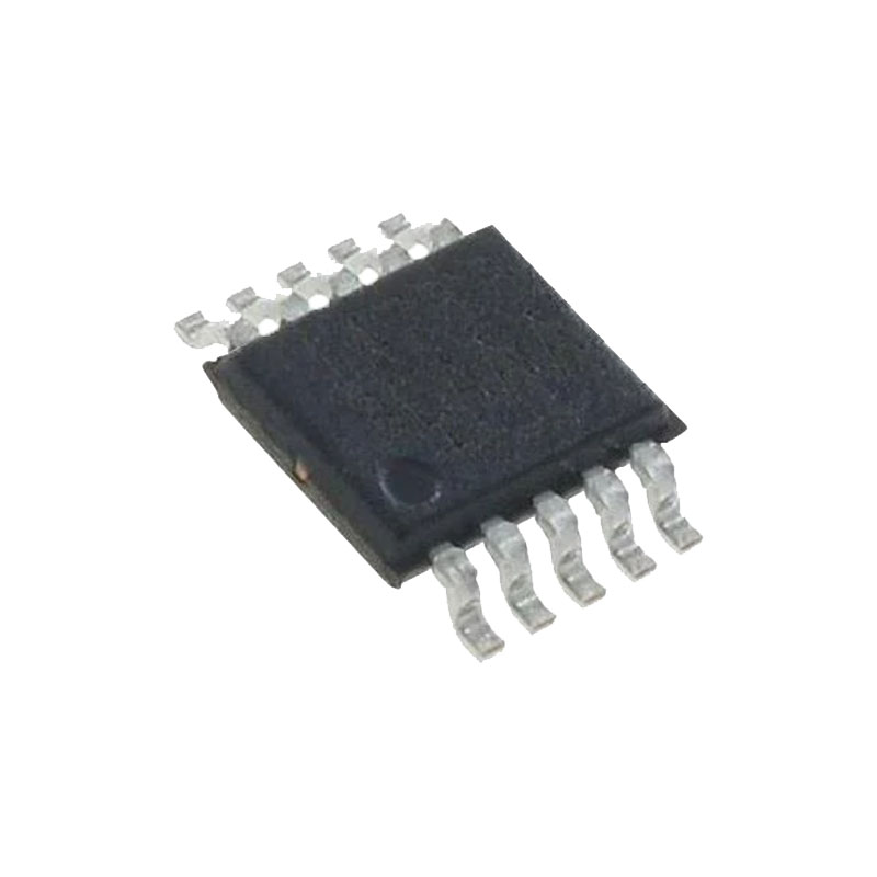
The MAX40263’s rail-to-rail input/outputs and low noise guarantee maximum dynamic range in demanding applications such as 12- to 14-bit SAR ADC drivers. Unlike traditional rail-to-rail input structures, input crossover distortion is absent due to an optimized input stage with an ultra-quiet charge pump. The input offset voltage is as low as 50μV due to the autocalibration performed during pow er-up. The device also includes a fast-power-on shutdown mode for further power savings. The MAX40263 operates from a wide supply range of 1.8V to 5.5V over the -40°C to +125°C temperature range and consumes only 750μA (typ) supply current per channel. It is available in a tiny, 10-pin QFN package.
The MAX40263 is an extension of the MAX44259/60/61/ 63 and MAX40110/11 families with individual shutdown pins for separate channels. 
Anwendungen
- Notebooks
- 3G/4G Handsets
- Portable Medical Instruments
- Battery-Operated Devices
- Analog-to-Digital Converter Buffers
- Transimpedance Amplifiers
- General-Purpose Signal Processing
Benefits and Features
- Wide Supply Range from 1.8V to 5.5V over the -40°C to +125°C Range
- Low 50μV (Max) Input Offset Voltage with Power-On Autocalibration at +25°C
- 15 MHz Unity-Gain Bandwidth
- Low 12.7nV/√Hz Input Voltage-Noise Density
- 750μA Quiescent Current per Channel
- Rail-to-Rail Inputs and Outputs
- <1.5pA Low Input Bias Current at +25°C
- Power-Saving Shutdown Mode
- Separate Shutdown for Each Channel
- Low 105dB Total Harmonic Distortion
- No Phase Reversal in Overdrive Conditions
Detaillierte Beschreibung
The MAX40263 is a high-speed, low-power dual-channel op-amp ideal for signal processing applications due to the device’s high precision and low-noise CMOS inputs. The device self-calibrates on power-up to eliminate the effects of temperature and power supply variation. Each channel of MAX40263 can enter into low-power shutdown mode separately and recover in 30μs.
Crossover Distortion
The device features a low-noise integrated charge pump that creates an internal voltage rail 1V above VDD, which powers the input differential pair of PMOS transistors. This unique architecture eliminates crossover distortion common in traditional CMOS input architecture, especially when used in a noninverting configuration such as Sallen-Key filters.
The charge pump operating frequency lies well above the unity-gain frequency of the amplifier. Because of its high frequency operation and ultra-quiet circuitry, the charge pump generates little noise, does not require external components, and is entirely transparent to the user.
Applications Information
Power-Up Autotrim
The MAX40263 features an automatic trim that self-calibrates the input offset voltage (VOS) to less than 50µV on power up. This self-calibration feature allows the device to eliminate input offset voltage effects due to power supply and operating temperature variation simply by cycling its power.
The device power-up speed should be fast to avoid the case when the self-calibration is triggered before the supply settles. Such a wrong condition would give an undesired large offset. To achieve targeted low VOS values, it is recommended to either (a) use a power supply with a fast slew rate (power supply settles in <10ms), or (b) power up the chip in the shutdown mode (SHDNA = SHDNB = low) and enable the chip (SHDNA = SHDNB = high) after the supply settles.
Shutdown Operation
The MAX40263 is a dual channel op-amp, and each channel of MAX40263 can enter into low-power shutdown mode separately by pulling down SHDNA or SHDNB.
Shutdown mode puts both inputs and outputs into high impedance and substantially lowers the quiescent current. Putting the output into high impedance allows multiple outputs to be multiplexed onto a single output line without the additional external buffers. The device does not self-calibrate when exiting shutdown mode and retains its power-up trim settings.
The shutdown logic levels of the device are independent of supply, allowing the shutdown feature of the device to operate off a 1.8V or 3.3V microcontroller, regardless of supply voltage.