Allgemeine Beschreibung
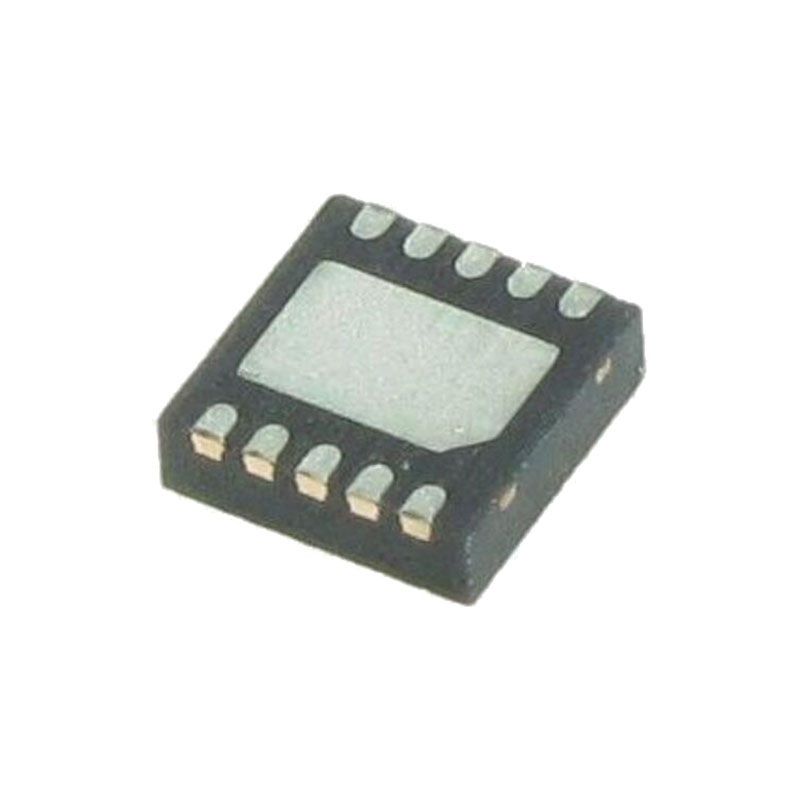
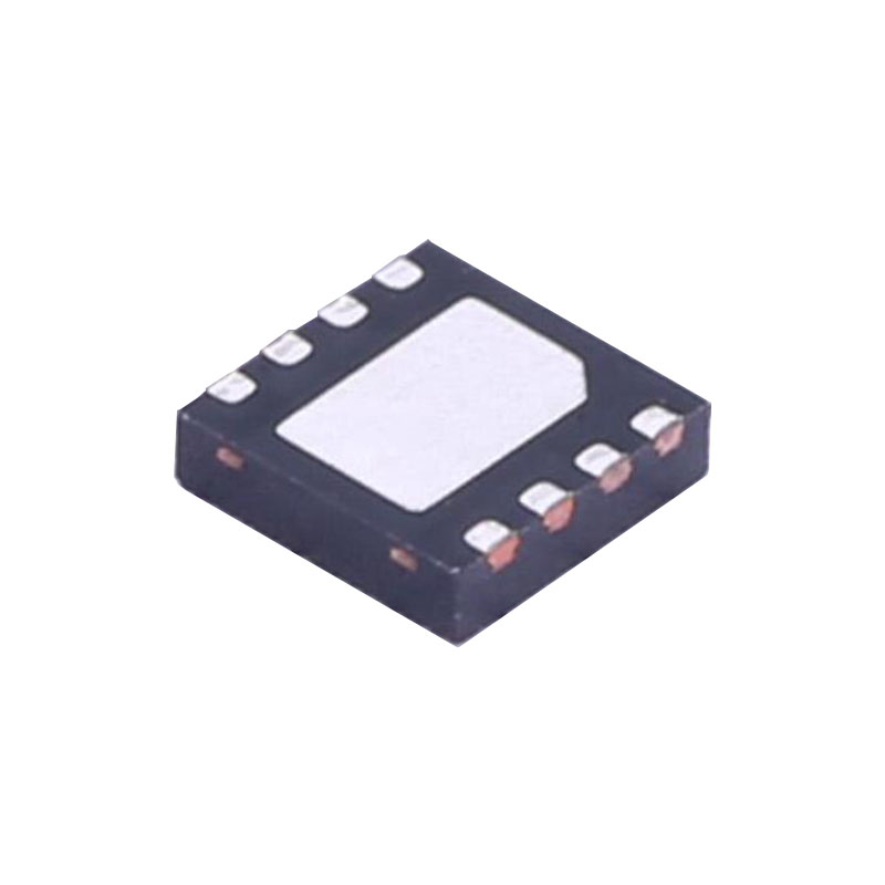
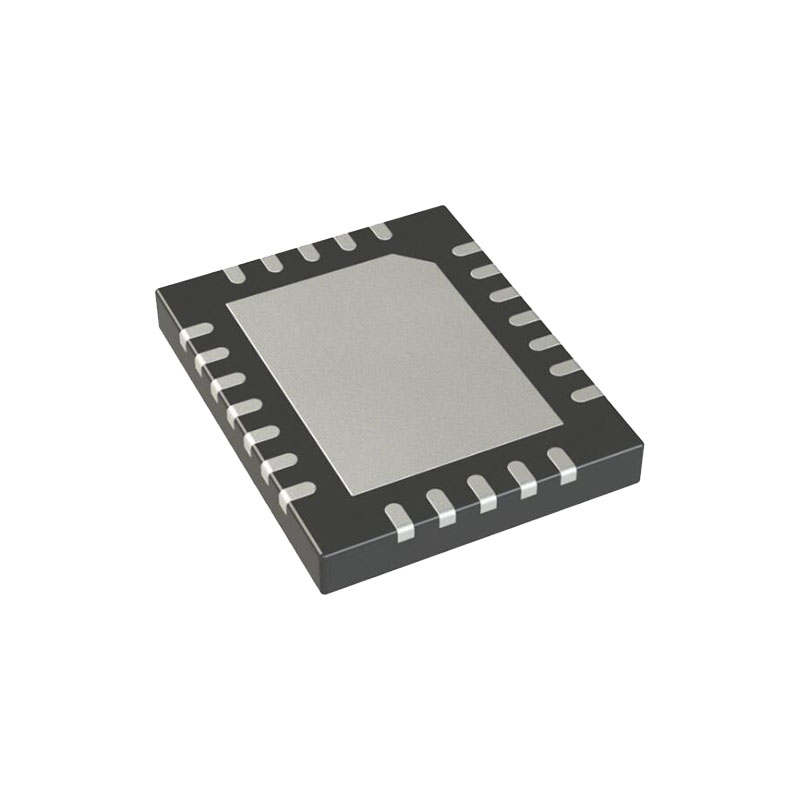
The MAX8794 DDR linear regulator sources and sinks up to 3A peak (typ) using internal n-channel MOSFETs. This linear regulator delivers an accurate 0.5V to 1.5V output from a low-voltage power input (VIN = 1.1V to 3.6V). The MAX8794 uses a separate 3.3V bias supply to power the control circuitry and drive the internal n-channel MOSFETs. The MAX8794 provides current and thermal limits to prevent damage to the linear regulator. Additionally, the MAX8794 generates a power-good (PGOOD) signal to indicate that the output is in regulation. During startup, PGOOD remains low until the output is in regulation for 2ms (typ). The internal soft-start limits the input surge current.The MAX8794 powers the active-DDR termination bus that requires a tracking input reference. The MAX8794 can also be used in low-power chipsets and graphics processor cores that require dynamically adjustable output voltages. The MAX8794 is available in a 10-pin, 3mm x 3mm, TDFN package.
Anwendungen
Notebook/Desktop Computers
DDR-Speicher Terminierung
Active Termination Buses
Graphics Processor Core Supplies
Chipset/RAM Supplies as Low as 0.5V
Detaillierte Beschreibung
The MAX8794 is a low-voltage, low-dropout DDR termination linear regulator with an external bias supply input and a buffered reference output. VCC is powered by a 2.7V to 3.6V supply that is commonly available in laptop and desktop computers. The 3.3V bias supply drives the gate of the internal pass transistor, while a lower voltage input at the drain of the transistor (IN) is regulated to provide VOUT. By using separate bias and power inputs, the MAX8794 can drive an n-channel highside MOSFET and use a lower input voltage to provide better efficiency.
The MAX8794 regulates its output voltage to the voltage at REFIN. When used in DDR applications as a termination supply, the MAX8794 delivers 1.25V or 0.9V at 3A peak (typ) from an input voltage of 1.1V to 3.6V. The MAX8794 sinks up to 3A peak (typ) as required in a termination supply. The MAX8794 provides shoot-through protection, ensuring that the source and sink MOSFETs do not conduct at the same time, yet produces a fast source-to-sink load transient.
The MAX8794 features an open-drain PGOOD output that transitions high 2ms after the output initially reaches regulation. PGOOD goes low within 10μs of when the output goes out of regulation by ±150mV. The MAX8794 features current- and thermal-limiting circuitry to prevent damage during fault conditions.
3.3V Bias Supply (VCC)
The VCC input powers the control circuitry and provides the gate drive to the pass transistor. This improves efficiency by allowing VIN to be powered from a lower supply voltage. Power VCC from a well-regulated 3.3V supply. Current drawn from the VCC supply remains relatively constant with variations in VIN and load current. Bypass VCC with a 1μF or greater ceramic capacitor as close to the device as possible.
VCC Undervoltage Lockout (UVLO)
The VCC input UVLO circuitry ensures that the regulator starts up with adequate voltage for the gate-drive circuitry to bias the internal pass transistor. The UVLO threshold is 2.55V (typ). VCC must remain above this level for proper operation.
Power-Supply Input (IN)
IN provides the source current for the linear regulator’s output, OUT. IN connects to the drain of the internal n-channel power MOSFET. IN can be as low as 1.1V, minimizing power dissipation. The input UVLO prohibits operation below 0.9V (typ). Bypass IN with a 10μF or greater capacitor as close to the device as possible.
Reference Input (REFIN)
The MAX8794 regulates OUTS to the voltage set at REFIN, making the MAX8794 ideal for memory applications where the termination supply must track the supply voltage. Typically, REFIN is set by an external resistive voltage-divider connected to the memory supply (VDDQ) .
The maximum output voltage of 1.5V is limited by the gatedrive voltage of the internal n-channel power transistor.

