ALLGEMEINE BESCHREIBUNG
The OP177 features one of the highest precision performance of any operational amplifier currently available. Offset voltage of the OP177 is only 25 μV maximum at room temperature. The ultralow VOS of the OP177 combines with the exceptional offset voltage drift (TCVOS) of 0.3 μV/°C maximum to eliminate the need for external VOS adjustment and increases system accuracy over temperature.
The OP177 open-loop gain of 12 V/μV is maintained over the full ±10 V output range. CMRR of 130 dB minimum, PSRR of 120 dB minimum, and maximum supply current of 2 mA are just a few examples of the excellent performance of this operational amplifier.
The combination of outstanding specifications of the OP177 ensures accurate performance in high closed-loop gain applications.
This low noise, bipolar input operational amplifier is also a cost effective alternative to chopper-stabilized amplifiers. The OP177 provides chopper-type performance without the usual problems of high noise, low frequency chopper spikes, large physical size, limited common-mode input voltage range, and bulky external storage capacitors.
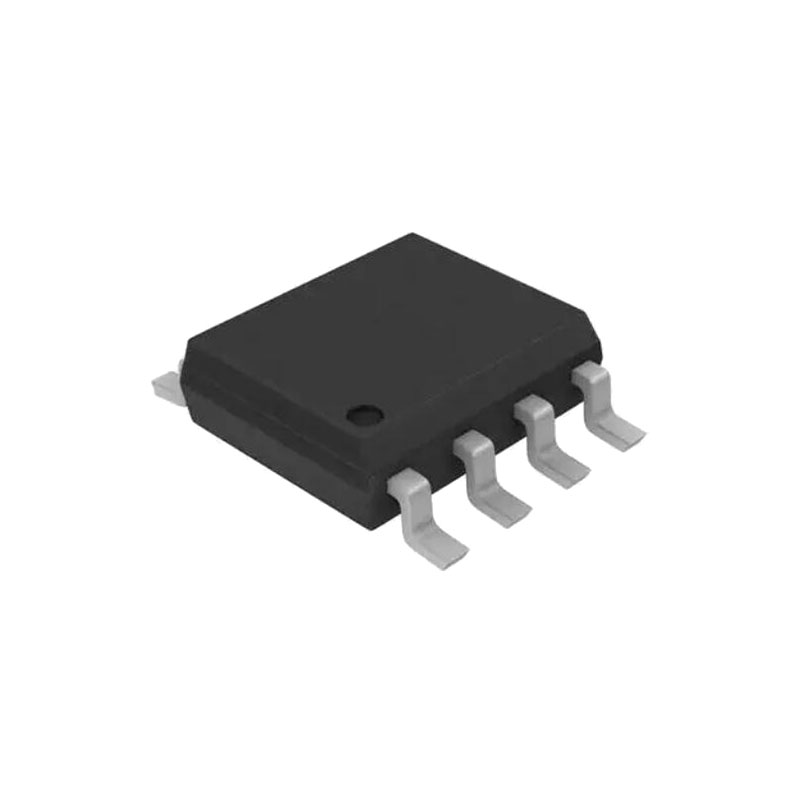
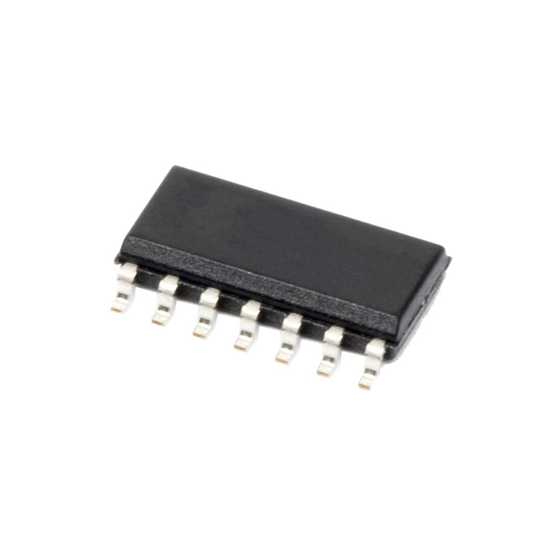
The OP177 is offered in the −40°C to +85°C extended industrial temperature ranges. This product is available in 8-lead PDIP, as well as the space saving 8-lead SOIC.
FEATURES
Ultralow offset voltage TA = 25°C, 25 μV maximum
Outstanding offset voltage drift 0.3 μV/°C maximum
Excellent open-loop gain and gain linearity 12 V/μV typical
CMRR: 130 dB minimum
PSRR: 115 dB minimum
Low supply current 2.0 mA maximum
Fits industry-standard precision operational amplifier sockets
WÄRMEBESTÄNDIGKEIT
θJA is specified for worst-case mounting conditions, that is, θJA is specified for device in socket for PDIP; θJA is specified for device soldered to printed circuit board for SOIC package.
ANWENDUNGSINFORMATIONEN
GAIN LINEARITY
The actual open-loop gain of most monolithic operational amplifiers varies at different output voltages. This nonlinearity causes errors in high closed-loop gain circuits.
It is important to know that the manufacturer’s AVO specification is only a part of the solution because all automated testers use endpoint testing and, therefore, show only the average gain. For example, However, the gain is not constant through the output voltage range, causing nonlinear errors. An ideal operational amplifier shows a horizontal scope trace.
THERMOCOUPLE AMPLIFIER WITH COLD JUNCTION COMPENSATION
An example of a precision circuit is a thermocouple amplifier that must accurately amplify very low level signals without introducing linearity and offset errors to the circuit. In this circuit, an S-type thermocouple with a Seebeck coefficient of 10.3 μV/°C produces 10.3 mV of output voltage at a temperature of 1000°C. The amplifier gain is set at 973.16, thus, it produces an output voltage of 10.024 V. Extended temperature ranges beyond 1500°C are accomplished by reducing the amplifier gain. The circuit uses a low cost diode to sense the temperature at the terminating junctions and, in turn, compensates for any ambient temperature change. The OP177, with the high openloop gain plus low offset voltage and drift, combines to yield a precise temperature sensing circuit.
PRECISION HIGH GAIN DIFFERENTIAL AMPLIFIER
The high gain, gain linearity, CMRR, and low TCVOS of the OP177 make it possible to obtain performance not previously available in single stage, very high gain amplifier applications.
ISOLATING LARGE CAPACITIVE LOADS
The reduces maximum slew rate but allows driving capacitive loads of any size without instability. Because the 100 Ω resistor is inside the feedback loop, the effect on output impedance is reduced to insignificance by the high open loop gain of the OP177.
PRECISION ABSOLUTE VALUE AMPLIFIER
The high gain and low TCVOS assure accurate operation with inputs from microvolts to volts. In this circuit, the signal always appears as a common-mode signal to the operational amplifiers.

