Beschreibung:
The S29GL01G/512/256/128S are MIRRORBIT™ Eclipse flash products fabricated on 65-nm process technology.These devices offer a fast page access time as fast as 15 ns with a corresponding random access time as fast as 90 ns. They feature a Write Buffer that allows a maximum of 256 words/512 bytes to be programmed in one operation, resulting in faster effective programming time than standard programming algorithms. This makes these devices ideal for today’s embedded applications that require higher density, better performance and lower power consumption.
Merkmale:
- CMOS 3.0 V core with versatile I/O
- 65 nm MIRRORBIT™ Eclipse technology
- Single supply (VCC) for read / program / erase (2.7 V to 3.6 V)
- Versatile I/O feature
– Wide I/O voltage range (VIO): 1.65 V to VCC
- ×16 data bus
- Asynchronous 32-byte page read
- 512-byte programming buffer
– Programming in page multiples, up to a maximum of 512 bytes
- Single word and multiple program on same word options
- Automatic error checking and correction (ECC) – internal hardware ECC with single bit error correction
- Sector erase
– Uniform 128-kbyte sectors
- Suspend and resume commands for program and erase operations
- Status register, data polling, and ready/busy pin methods to determine device status
- Advanced sector protection (ASP)
– Volatile and non-volatile protection methods for each sector
- Separate 1024-byte one time program (OTP) array with two lockable regions
- Common flash interface (CFI) parameter table
- Temperature range / grade
– Industrial (–40°C to +85°C)
- 100,000 program / erase cycles
- 20 years data retention
- Packaging options
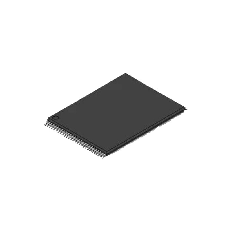
– 56-pin TSOP
Product overview:
The GL-S family consists of 128-Mb to 1-Gb, 3.0 V core, versatile I/O, non-volatile, flash memory devices. These devices have a 16-bit (word) wide data bus and use only word boundary addresses. All read accesses provide 16 bits of data on each bus transfer cycle. All writes take 16 bits of data from each bus transfer cycle.
The GL-S family combines the best features of eXecute-In-Place (XIP) and data storage flash memories. This family has the fast random access of XIP flash along with the high density and fast program speed of Data Storage flash.
Read access to any random location takes 90 ns to 120 ns depending on device density and I/O power supply voltage. Each random (initial) access reads an entire 32-byte aligned group of data called a page. Other words within the same page may be read by changing only the low order 4 bits of word address. Each access within the same page takes 15 ns to 30 ns. This is called page mode read. Changing any of the higher word address bits will select a different page and begin a new initial access. All read accesses are asynchronous.
S29GL-S address map:
The device control logic is subdivided into two parallel operating sections, the host interface controller (HIC) and the embedded algorithm controller (EAC). HIC monitors signal levels on the device inputs and drives outputs as needed to complete read and write data transfers with the host system. HIC delivers data from the currently entered address map on read transfers; places write transfer address and data information into the EAC command memory; notifies the EAC of power transition, hardware reset, and write transfers. The EAC looks in the command memory, after a write transfer, for legal command sequences and performs the related embedded algorithms.
Changing the non-volatile data in the memory array requires a complex sequence of operations that are called embedded algorithms (EA). The algorithms are managed entirely by the device internal EAC. The main algorithms perform programming and erase of the main array data. The host system writes command codes to the flash device address space. The EAC receives the commands, performs all the necessary steps to complete the command, and provides status information during the progress of an EA.

