Beschreibung
The THS3091 and THS3095 (THS309x) are high-voltage, low-distortion, high-speed, current-feedback amplifiers that operate over a wide supply range of ±5 V to ±16 V. These devices are an excellent choice for applications that require large, linear output signals, such as pin drivers, power-FET drivers, and arbitrary waveform generators.
The THS3095 features a power-down pin (PD) that puts the amplifier into a low-power standby mode, and lowers the quiescent current from 9.5 mA to 500 μA.
The wide, 32-V supply range, 6000-V/µs slew rate, and 310-mA output current drive make the THS309x an excellent choice for high-voltage arbitrary-waveform-driver applications. Moreover, with the ability to handle large voltage swings driving into low-resistance and high-capacitance loads while maintaining good settling time performance, these devices are an excellent choice for pin-driver and power-FET driver applications.
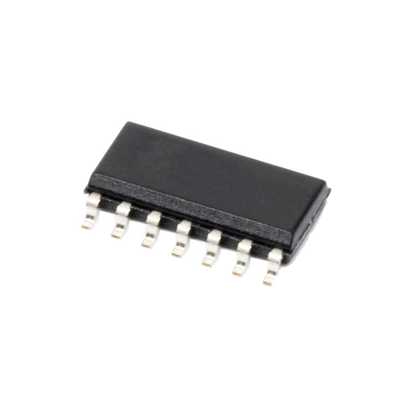
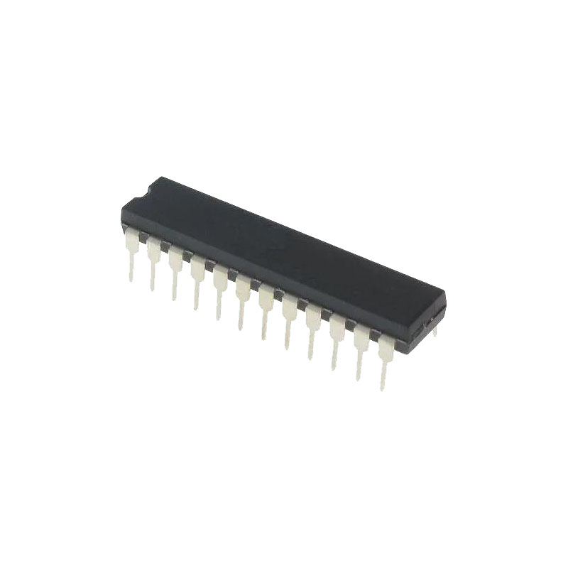
The THS309x are offered in an 8-pin SOIC (DDA) PowerPAD™ integrated circuit package. The THS3091 is also offered in an 8-pin HVSSOP (DGN) package.
Eigenschaften
• Low distortion:
– 84-dBc HD2 at 10 MHz, RL = 1 kΩ
– 99-dBc HD3 at 10 MHz, RL = 1 kΩ
• Low noise
• High slew rate: 6000 V/μs (G = 5, VO = 20 VPP)
• Wide bandwidth: 305 MHz (G = 2, RL = 100 Ω)
• High output current drive: ±310 mA
• Wide supply range: ±5 V to ±16 V
• Power-down feature: THS3095 only
Anwendungen
• High-voltage arbitrary waveform generators
• Pin Driver
• Power-FET drivers
• Source measurement unit (SMU)
• High capacitive load piezo element drivers
Übersicht
The THS3091 and THS3095 (THS309x) are high-voltage, low-distortion, high-speed, current feedback amplifiers. The THS309x are designed to operate over a wide supply range of ±5 V to ±16 V for applications requiring large, linear output swings, such as arbitrary waveform generators.
The THS3095 also features a power-down pin that puts the amplifier into a low-power standby mode, and lowers the quiescent current from 9.5 mA to 500 µA.
Wideband, Noninverting Operation
The THS309x are unity gain stable 715-MHz current-feedback operational amplifiers designed to operate from a ±5-V to ±15-V power supply. Most of the curves were characterized using signal sources with a 50-Ω source impedance, and with measurement equipment presenting a 50-Ω load impedance.
Typical Application
The fundamental concept of load sharing is to drive a load using two or more of the same operational amplifiers. Each amplifier is driven by the same source. This concept effectively reduces the current load of each amplifier by 1/N, where N is the number of amplifiers. For further details on the design and performance of this circuit, see the Reference Design for Implementation of the Load Sharing Concept for Large-Signal Applications.
Detailed Design Procedure
In addition to providing higher output current drive to the load, the load sharing configuration can also provide improved distortion performance. In many cases, an operational amplifier shows better distortion performance as the load current decreases (that is, for higher resistive loads) until the feedback resistor starts to dominate the current load. In a load sharing configuration of N amplifiers in parallel, the equivalent current load that each amplifier drives is 1/N times the total load current.
Power Supply Recommendations
The THS3091 operates using a single or dual supply as long as the input CM voltage range (CMIR) has the required headroom to either supply rail. Operating from a single supply has numerous advantages. With the negative supply at ground, the dc errors due to the –PSRR term are minimized. Decouple the supplies with low-inductance, ceramic capacitors to ground less than 0.5 inches from the device pins. The use of a ground plane is recommended; as in most high-speed devices, remove the ground plane near device sensitive pins such as the inputs. For split-supply operation, an optional supply decoupling capacitor across the two power supplies improves second harmonic distortion performance.