DESCRIPCIÓN
The LTC4234 is an integrated solution for Hot Swap™ applications that allows a board to be safely inserted and removed from a live backplane. The part integrates a Hot Swap controller, power MOSFET and current sense resistor in a single package for small form factor applications. The MOSFET Safe Operating Area is production tested and guaranteed for the stresses in Hot Swap applications.
The LTC4234 provides separate inrush current control and an 11% accurate 22.5A current limit with output dependent foldback. The current limit threshold can be adjusted dynamically using the ISET pin. Additional features include a current monitor output that amplifies the sense resistor voltage for ground referenced current sensing and a MOSFET temperature monitor output. Thermal limit, overvoltage, undervoltage and power good monitoring are also provided. For a 10A compatible version, see LTC4233.
CARACTERÍSTICAS
Allows Safe Board Insertion into Live Backplane
Small Footprint
4mΩ MOSFET Including RSENSE
Safe Operating Area Guaranteed at 81W, 30ms
Wide Operating Voltage Range: 2.9V to 15V
Adjustable, 11% Accurate Current Limit
Current and Temperature Monitor Outputs
Protección contra sobretemperatura
Adjustable Current Limit Timer Before Fault
Power Good and Fault Outputs
Adjustable Inrush Current Control
2.5% Accurate Undervoltage and Overvoltage Protection
Pin Compatible with LTC4233
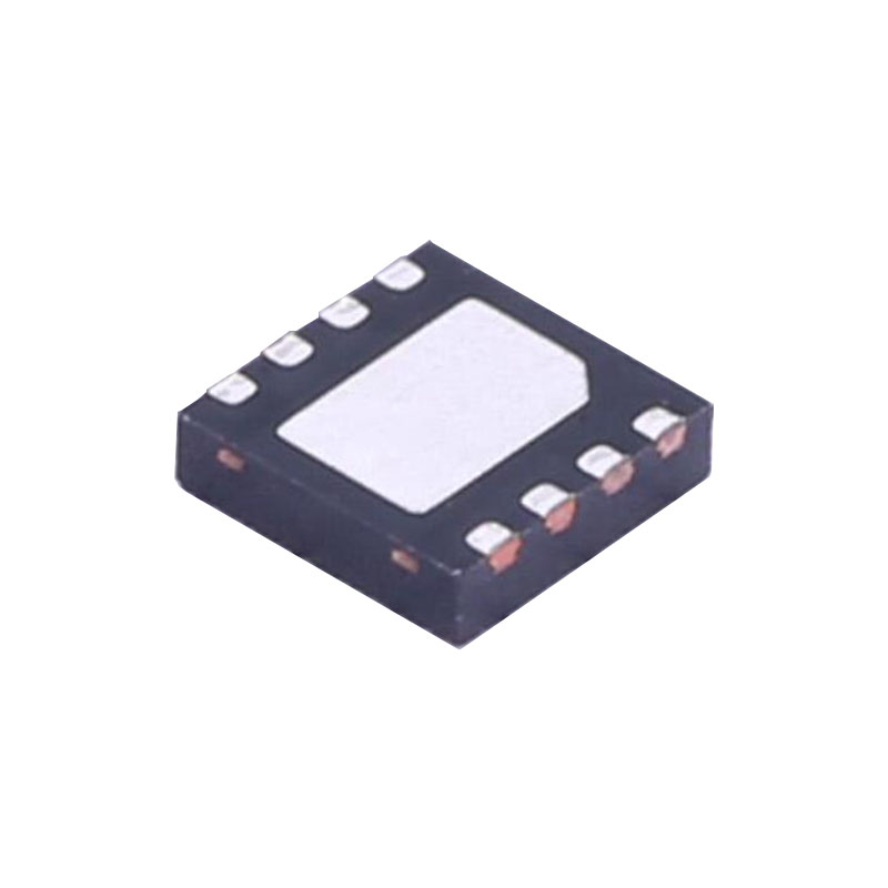
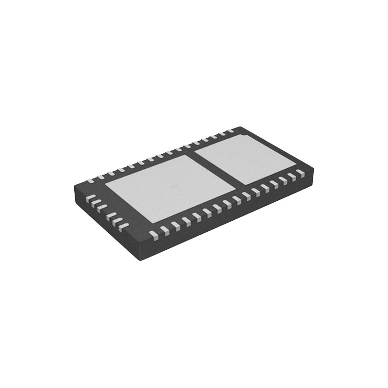
Available in a 38-Pin (5mm × 9mm) QFN Package
APLICACIONES
High Availability Servers
Solid State Drives
Industrial
240W, 12V Systems
OPERACIÓN
The Functional Diagram displays the main circuits of the device. The LTC4234 is designed to turn a board’s supply voltage on and off in a controlled manner allowing the board to be safely inserted and removed from a live backplane. The LTC4234 includes a 3.3mΩ MOSFET and a 0.7mΩ current sense resistor. During normal operation, the charge pump and gate driver turn on the pass MOSFET’s gate to provide power to the load. The inrush current control is accomplished by the INRUSH circuit. This circuit limits the GATE ramp rate to 0.35V/ms and hence controls the voltage ramp rate of the output capacitor.
The current sense (CS) amplifier monitors the load current using the voltage sensed across the current sense resistor. The CS amplifier limits the current in the load by reducing the GATE-to-OUT voltage in an active control loop. It is simple to adjust the current limit threshold using the current limit adjustment (ISET) pin. This allows a different threshold during other times such as start-up. Note there must be a connection between SENSE to SENSE− (Pin 34 to Pin 31) in order to monitor current.
A short circuit on the output to ground causes significant power dissipation during active current limiting. To limit this power, the foldback amplifier reduces the current limit value from 22.5A to 5.7A in a linear manner as the FB pin drops below 0.6V (see the Typical Performance Characteristics).
If an overcurrent condition persists, the TIMER pin ramps up with a 100µA current source until the pin voltage exceeds 1.235V (comparator TM2). This indicates to the logic that it is time to turn off the pass MOSFET to prevent overheating. At this point the TIMER pin ramps down using the 2µA current source until the voltage drops below 0.21V (Comparator TM1) which completes one timer cycle. After eight TIMER pin cycles (ramping to 1.235V and then below 0.21V) the logic starts the internal 48ms timer. At this point, the pass transistor has cooled and it is safe to turn it on again. It is suitable in many applications to use an internal 2ms overcurrent timer with a 900ms cool down period. Tying the TIMER pin to INTVCC sets this default timing. Latchoff is the normal operating condition following overcurrent turnoff. Retry is initiated by pulling the UV pin low for a minimum of 1µs then high. Auto-retry is implemented by tying the FLT to the UV pin.
INFORMACIÓN SOBRE APLICACIONES
The typical LTC4234 application is in a high availability system that uses a positive voltage supply to distribute power to individual cards.
Turn-On Sequence
Several conditions must be present before the internal pass MOSFET can be turned on. First the supply VDD must exceed its undervoltage lockout level. Next the internally generated supply INTVCC must cross its 2.65V undervoltage threshold. This generates a 25µs power-on-reset pulse which clears the fault register and initializes internal latches.
After the power-on-reset pulse, the UV and OV pins must indicate that the input voltage is within the acceptable range. All of these conditions must be satisfied for a duration of 48ms to ensure that any contact bounce during the insertion has ended.