Descripción:
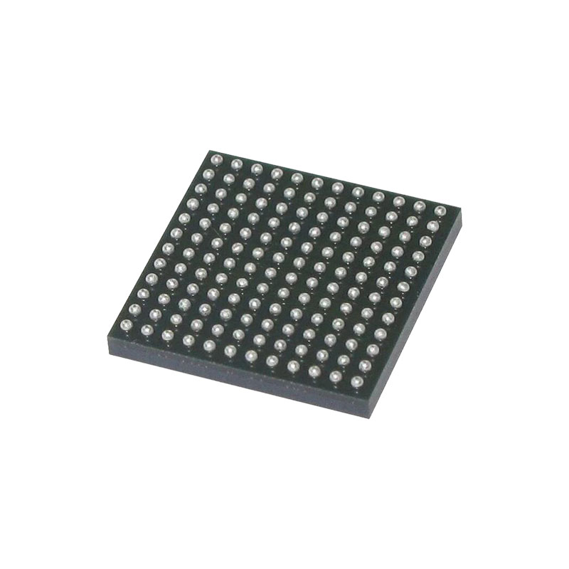
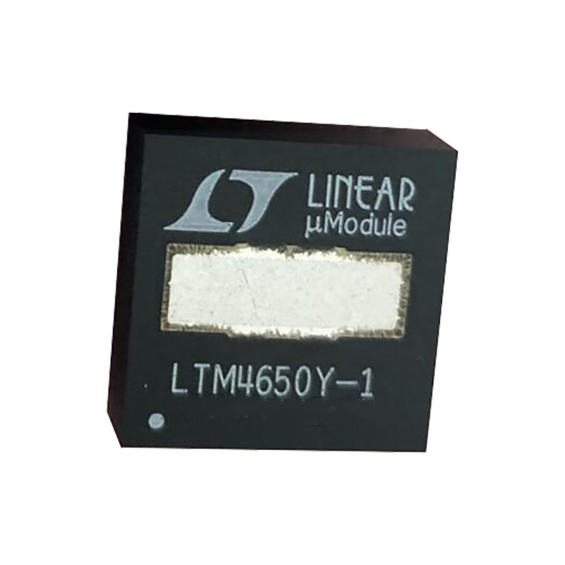
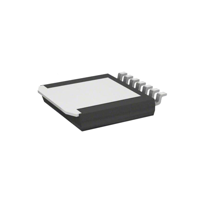
The LTM4650-1A/LTM4650-1B is dual 25A or single 50A output step-down µModule® (power module) regulator with ±0.8% (LTM4650-1A) and ±1.5% (LTM4650-1B) total DC output error with ±3% transient output error. Included in the package are the switching controller, power FETs, inductors, and all supporting components. External compensation allows for fast transient response to minimize output capacitance when powering FPGAs, ASICs, and processors. With synchronized multiphase parallel current sharing, six LTM4650-1 devices can deliver up to 300A. The LTM4650-1 is offered in a 16mm × 16mm × 5.01 BGA package, with SnPb (BGA) or RoHS compliant terminal finish.
Características:
±0.8% Maximum Total DC Output Error Over Line and Load (LTM4650-1A)
±3% Transient Output Error with Minimum Output Capacitance
Dual 25A or Single 50A Output
Entrada de 4,5 V a 15 V, rango de tensión de salida de 0,6 V a 1,8 V
Amplificador diferencial de teledetección
Control en modo corriente/Respuesta rápida a transitorios
Current Sharing Up to 300A
Aplicaciones:
FPGA, ASIC, μRegulación de la tensión del núcleo del procesador
Sistemas de información y comunicación
ELECTRICAL CHARACTERISTICS NOTE
Pad or ball finish code is per IPC/JEDEC J-STD-609.
Las tensiones superiores a las indicadas en los valores nominales máximos absolutos pueden provocar daños permanentes en el dispositivo. La exposición a cualquier condición de máxima tensión absoluta durante periodos prolongados puede afectar a la fiabilidad y la vida útil del dispositivo.
The LTM4650-1 is tested under pulsed load conditions such that TJ ≈ TA. The LTM4650-1E is guaranteed to meet specifications from 0°C to 125°C internal temperature. Specifications over the –40°C to 125°C internal operating temperature range are assured by design, characterization and correlation with statistical process controls. The LTM4650-1I is guaranteed over the full –40°C to 125°C internal operatingtemperature range. Note that the maximum ambient temperature consistent with these specifications is determined by specific operating conditions in conjunction with board layout, the rated package thermal impedance and other environmental factors.
Two outputs are tested separately and the same testing condition is applied to each output.
LTM4650-1 device is designed to operate from 400kHz to 750kHz
These parameters are tested at wafer sort.
See output current derating curves for different VIN, VOUT and TA.
FUNCIONES DEL PIN
Recommended to use test points to monitor signal pin connections.
VOUT1 (A1-A5, B1-B5, C1-C4): Power Output Pins. Apply output load between these pins and GND pins. Recommend placing output decoupling capacitance directly between these pins and GND pins.
GND (A6-A7, B6-B7, D1-D4, D9-D12, E1-E4, E10-E12, F1-F3, F10-F12, G1, G3, G10, G12, H1-H7, H9-H12, J1, J5, J8, J12, K1, K5-K8, K12, L1, L12, M1 , M12): Power Ground Pins for Both Input and Output Returns.
VOUT2 (A8-A12, B8-B12, C9-C12): Power Output Pins. Apply output load between these pins and GND pins. Recommend placing output decoupling capacitance directly between these pins and GND pins.
VOUTS1, VOUTS2 (C5, C8): This pin is connected to the top of the internal top feedback resistor for each output. The pin can be directly connected to its specific output, or connected to DIFFOUT when the remote sense amplifier is used. In paralleling modules, one of the VOUTS pins is connected to the DIFFOUT pin in remote sensing or directly to VOUT with no remote sensing. It is very important to connect these pins to either the DIFFOUT or VOUT since this is the feedback path, and cannot be left open. See the Applications Information section.

