Descripción
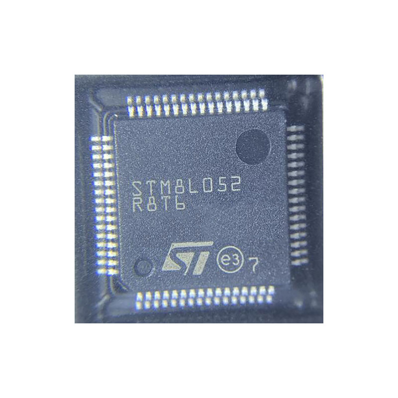
The value line STM8L05xxx ultra low power family features the enhanced STM8 CPU core providing increased processing power (up to 16 MIPS at 16 MHz) while maintaining the advantages of a CISC architecture with improved code density, a 24-bit linear addressing space and an optimized architecture for low power operations.
The family includes an integrated debug module with a hardware interface (SWIM) which allows non-intrusive In-application debugging and ultra-fast Flash programming.
High density value line STM8L05xxx microcontrollers feature embedded data EEPROM and low-power, low-voltage, single-supply program Flash memory.
All devices offer 12-bit ADC, real-time clock, four 16-bit timers, one 8-bit timer as well as standard communication interface such as two SPIs, I2C, three USARTs and 8×24 or 4×28- segment LCD. The 8×24 or 4x 28-segment LCD is available on the high density value line STM8L05xxx.
The STM8L05xxx family operates from 1.8 V to 3.6 V and is available in the -40 to +85 °C temperature range.
The modular design of the peripheral set allows the same peripherals to be found in different ST microcontroller families including 32-bit families. This makes any transition to a different family very easy, and simplified even more by the use of a common set of development tools.
All value line STM8L ultra low power products are based on the same architecture with the same memory mapping and a coherent pinout.
Características:
• Operating conditions
– Operating power supply: 1.8 V to 3.6 V
– Temperature range: -40 °C to 85 °C
• Low power features
– 5 low power modes: Wait, Low power run (5.9 µA), Low power wait (3 µA), Active-halt with full RTC (1.4 µA), Halt (400 nA)
– Dynamic power consumption: 200 µA/MHz + 330 µA
– Ultra-low leakage per I/0: 50 nA
– Fast wakeup from Halt: 4.7 µs
• Advanced STM8 core
– Harvard architecture and 3-stage pipeline
– Max freq. 16 MHz, 16 CISC MIPS peak
– Up to 40 external interrupt sources
• Reset and supply management
– Low power, ultra-safe BOR reset with 5 programmable thresholds
– Ultra low power POR/PDR
– Programmable voltage detector (PVD)
• Clock management
– 32 kHz and 1 to 16 MHz crystal oscillators
– Internal 16 MHz factory-trimmed RC
– 38 kHz low consumption RC
– Clock security system
• Low power RTC
– BCD calendar with alarm interrupt
– Digital calibration with +/- 0.5ppm accuracy
– Advanced anti-tamper detection
• LCD: 8×24 or 4×28 w/ step-up converter
• Memories
– 64 KB Flash program memory and 256 bytes data EEPROM with ECC, RWW
– Flexible write and read protection modes
– 4 KB of RAM
DMA
– 4 channels supporting ADC, SPIs, I2C, USARTs, timers
– 1 channel for memory-to-memory
• 12-bit ADC up to 1 Msps/27 channels
– Internal reference voltage
• Timers
– Three 16-bit timers with 2 channels (used as IC, OC, PWM), quadrature encoder
– One 16-bit advanced control timer with 3 channels, supporting motor control
– One 8-bit timer with 7-bit prescaler
– 2 watchdogs: 1 Window, 1 Independent
– Beeper timer with 1, 2 or 4 kHz frequencies
• Communication interfaces
– Two synchronous serial interfaces (SPI)
– Fast I2C 400 kHz SMBus and PMBus
– Three USARTs (ISO 7816 interface + IrDA)
• Up to 54 I/Os, all mappable on interrupt vectors
• Development support
– Fast on-chip programming and nonintrusive debugging with SWIM
– Bootloader using USART
Performance
All families incorporate highly energy-efficient cores with both Harvard architecture and pipelined execution: advanced STM8 core for STM8L families and ARM Cortex™-M3 core for STM32L family. In addition specific care for the design architecture has been taken to optimize the mA/DMIPS and mA/MHz ratios.
This allows the ultra low power performance to range from 5 up to 33.3 DMIPs.
Shared peripherals
STM8L05x, STM8L15x and STM32L15xx share identical peripherals which ensure a very easy migration from one family to another:
• Analog peripheral: ADC1
• Digital peripherals: RTC and some communication interfaces

