DESCRIPCIÓN GENERAL
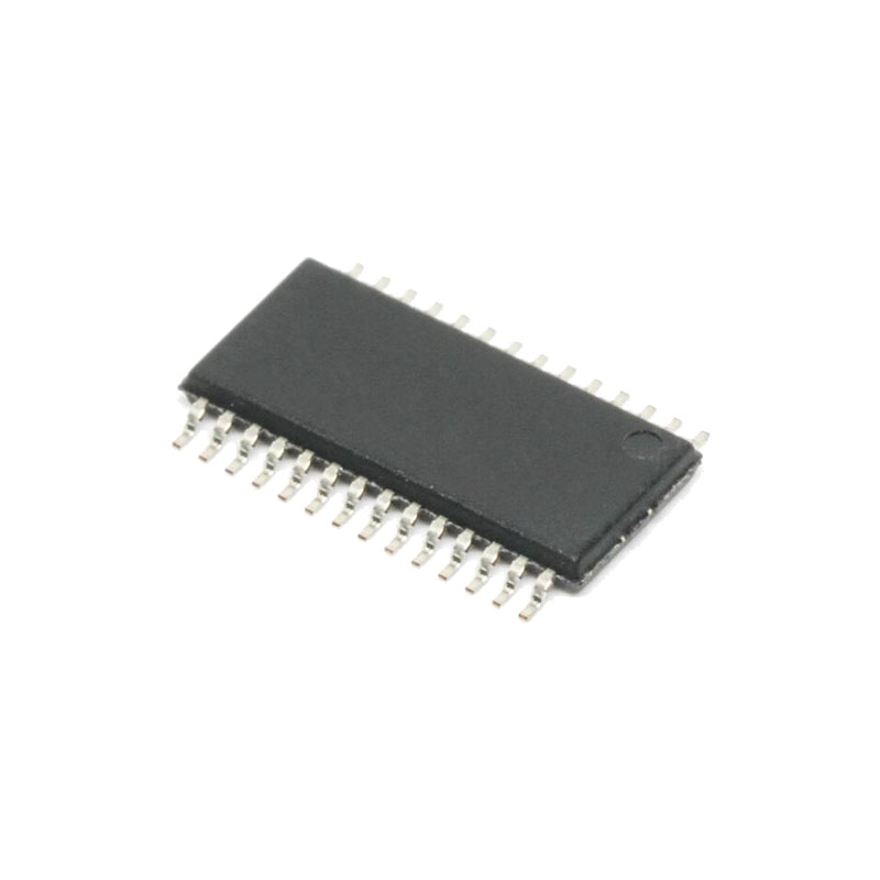
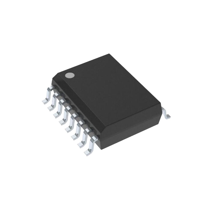
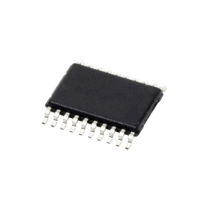
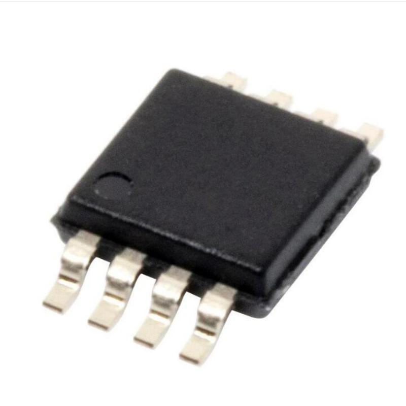
The AD7304 are quad, 8-bit DACs that operate from a single +3 V to +5 V supply, or ±5 V supplies. The AD7304 has a serial interface.Internal precision buffers swing rail-to-rail. The reference input range includes both supply rails, allowing for positive or negative full-scale output voltages. Operation is guaranteed over the supply voltage range of 2.7 V to 5.5 V, consuming less than 9 mW from a 3 V supply. The full-scale voltage output is determined by the external reference input voltage applied. The rail-to-rail VREF input to DAC VOUT allows for a full-scale voltage set equal to the positive supply, VDD, the negative supply, VSS, or any value in between. The AD7304’s doubled-buffered serial data interface offers high speed, 3-wire, SPI-, and microcontroller-compatible inputs using data in (SDI), clock (CLK), and chip select (CS) pins. Additionally, an internal power-on reset sets the output to zero scale. The parallel input AD7305 uses a standard address decode along with the WR control line to load data into the input registers. The double-buffered architecture allows all four input registers to be preloaded with new values, followed by an LDAC control strobe that copies all the new data into the DAC registers, thereby updating the analog output values.When operating from less than 5.5 V. An internal power-on reset places both parts in the zero-scale state at turn-on. A 40 µA power shutdown (SHDN) feature is activated on both parts by three-stating the SDI/SHDN pin on the AD7304 . The AD7304 are specified over the extended industrial −40°C to +85°C and the automotive −40°C to +125°C temperature ranges. AD7304s are available in a wide-body 16-lead SOIC (R-16) package. For ultracompact applications, the thin 1.1 mm, 16-lead TSSOP (RU-16) package is available for the AD7304.
CARACTERÍSTICAS
Four 8-bit DACs in one package
+3 V, +5 V, and ±5 V operation
Rail-to-rail REF input to voltage output swing
2.6 MHz reference multiplying bandwidth
Internal power-on reset
SPI serial interface-compatible—AD7304
40 µA power shutdown
APLICACIONES
Automotive output span voltage
Instrumentation, digitally controlled calibration
Pin-compatible AD7226 replacement when VDD < 5.5 V
CIRCUIT OPERATION
The AD7304 is 4-channel, 8-bit, voltage output DACs, differing primarily in digital logic interface and number of reference inputs. Both parts share the same internal DAC design and true rail-to-rail output buffers. The AD7304 contains four independent multiplying reference inputs. The AD7304 uses a 3-wire SPI-compatible serial data interface.
APLICACIONES
The AD7304/AD7305 are inherently 2-quadrant multiplying DACs. That is, they can easily be set up for unipolar output operation. The full-scale output polarity is the same as the reference input voltage polarity. In some applications, it may be necessary to generate the full 4-quadrant multiplying capability or a bipolar output swing. This is easily accomplished using an external true rail-to-rail op amp, such as the OP295. Connecting the external amplifier with
two equal value resistors, as shown in Figure 38, results in a full 4-quadrant multiplying circuit. In this circuit, the amplifier provides a gain of two, which increases the output span magnitude to 10 V. The transfer equation of this circuit shows that both negative and positive output voltages are created as the input data (D) is incremented from code zero (VOUT = –5 V)to midscale (VOUT = 0 V) to full scale (VOUT = +5 V).
PRECAUCIÓN ESD
ESD (electrostatic discharge) sensitive device. Electrostatic charges as high as 4000 V readily accumulate on the human body and test equipment and can discharge without detection. Although this product features proprietary ESD protection circuitry, permanent damage may occur on devices subjected to high energy electrostatic discharges. Therefore, proper ESD precautions are recommended to avoid performance degradation or loss of functionality

