DESCRIPCIÓN GENERAL
The AD8226 is a low cost, wide supply range instrumentation amplifier that requires only one external resistor to set any gain between 1 and 1000.
The AD8226 is designed to work with a variety of signal voltages. A wide input range and rail-to-rail output allow the signal to make full use of the supply rails. Because the input range also includes the ability to go below the negative supply, small signals near ground can be amplified without requiring dual supplies. The AD8226 operates on supplies ranging from ±1.35 V to ±18 V for dual supplies and 2.2 V to 36 V for single supply.
The robust AD8226 inputs are designed to connect to realworld sensors. In addition to its wide operating range, the AD8226 can handle voltages beyond the rails. For example, with a ±5 V supply, the part is guaranteed to withstand ±35 V at the input with no damage. Minimum as well as maximum input bias currents are specified to facilitate open wire detection.
The AD8226 is perfect for multichannel, space-constrained industrial applications. Unlike other low cost, low power instrumentation amplifiers, the AD8226 is designed with a minimum gain of 1 and can easily handle ±10 V signals. With its MSOP package and 125°C temperature rating, the AD8226 thrives in tightly packed, zero airflow designs.
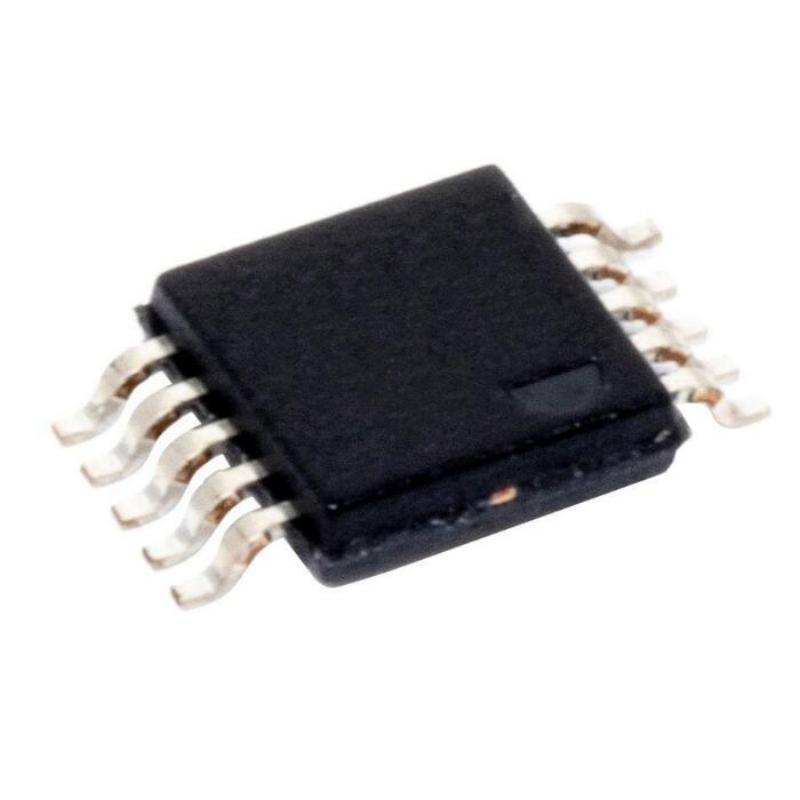
The AD8226 is available in 8-lead MSOP and SOIC packages, and is fully specified for −40°C to +125°C operation.
For a device with a similar package and performance as the AD8226 but with gain settable from 5 to 1000, consider using the AD8227.
CARACTERÍSTICAS
Gain set with 1 external resistor Gain range: 1 to 1000
Input voltage goes below ground
Inputs protected beyond supplies
Very wide power supply range
Single supply: 2.2 V to 36 V
Dual supplies: ±1.35 V to ±18 V
Bandwidth (G = 1): 1.5 MHz
CMRR (G = 1): 90 dB minimum for BR models
Input noise: 22 nV/√Hz
Typical supply current: 350 μA
Specified temperature: −40°C to +125°C
8-lead SOIC and MSOP packages
APLICACIONES
Industrial process controls
Bridge amplifiers
Instrumentación médica
Portable data acquisition
Multichannel systems
REFERENCE TERMINAL
The output voltage of the AD8226 is developed with respect to the potential on the reference terminal. This is useful when the output signal needs to be offset to a precise midsupply level. For example, a voltage source can be tied to the REF pin to levelshift the output so that the AD8226 can drive a single-supply ADC. The REF pin is protected with ESD diodes and should not exceed either +VS or −VS by more than 0.3 V.
Performance Across Temperature
The common-mode input range shifts upward with temperature. At cold temperatures, the part requires extra headroom from the positive supply, and operation near the negative supply has more margin. Conversely, hot temperatures require less headroom from the positive supply, but are the worst-case conditions for input voltages near the negative supply.
Recommendation for Best Performance
A typical part functions up to the boundaries described in this section. However, for best performance, designing with a few hundred millivolts extra margin is recommended. As signals approach the boundary, internal transistors begin to saturate, which can affect frequency and linearity performance.
If the application requirements exceed the boundaries, one solution is to apply less gain with the AD8226, and then apply additional gain later in the signal chain. Another option is to use the pin-compatible AD8227.
LAYOUT
To ensure optimum performance of the AD8226 at the PCB level, care must be taken in the design of the board layout.
The AD8226 pins are arranged in a logical manner to aid in this task.