Descripción:
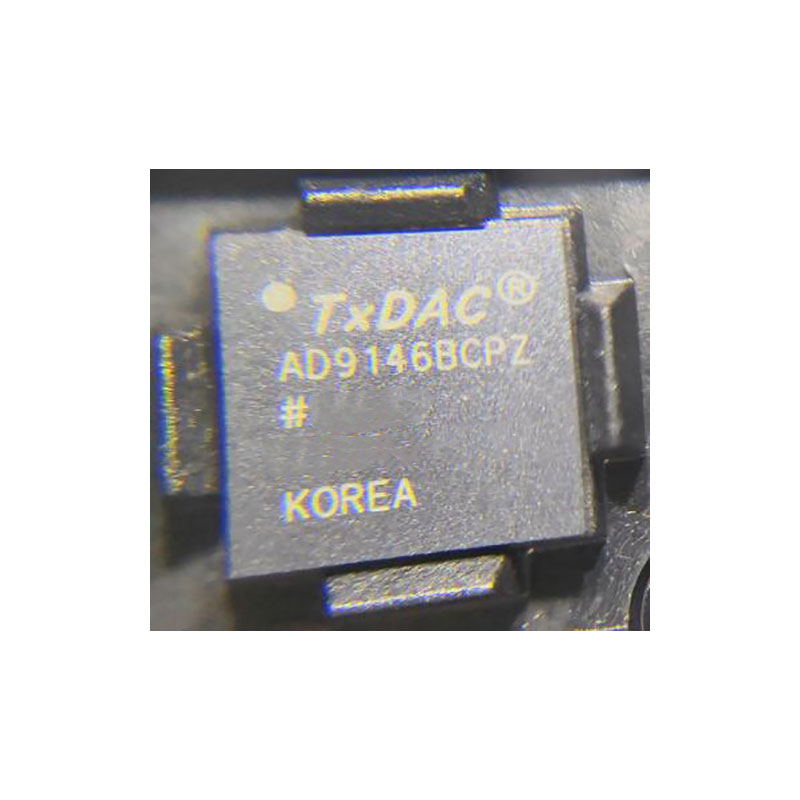
The AD9146BCPZ is a dual, high dynamic range digital-to-analog converter (DAC) that provides a sample rate of 1230 MSPS, permitting multicarrier generation up to the Nyquist frequency.
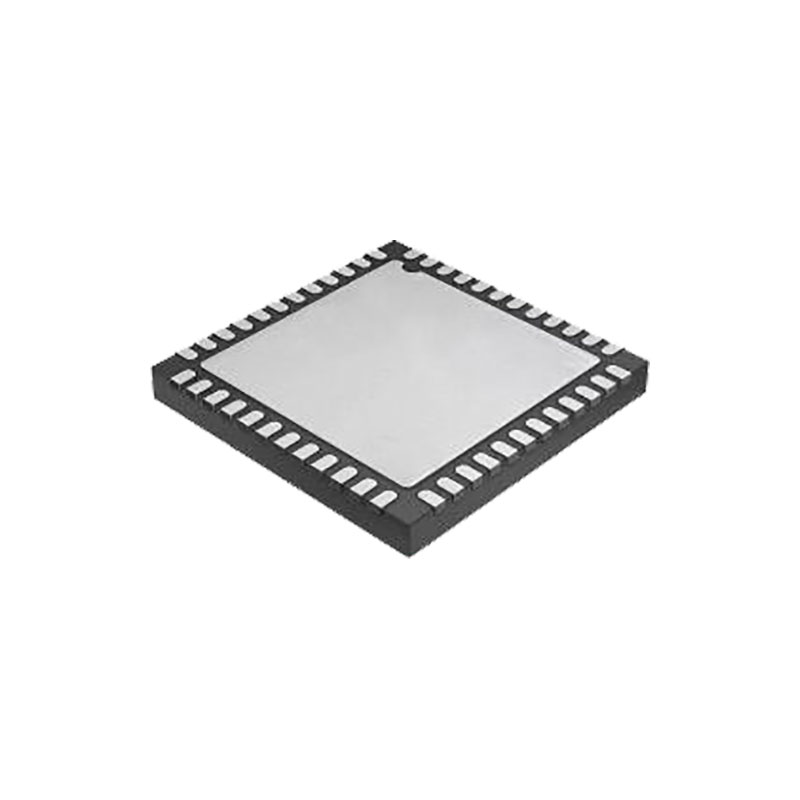
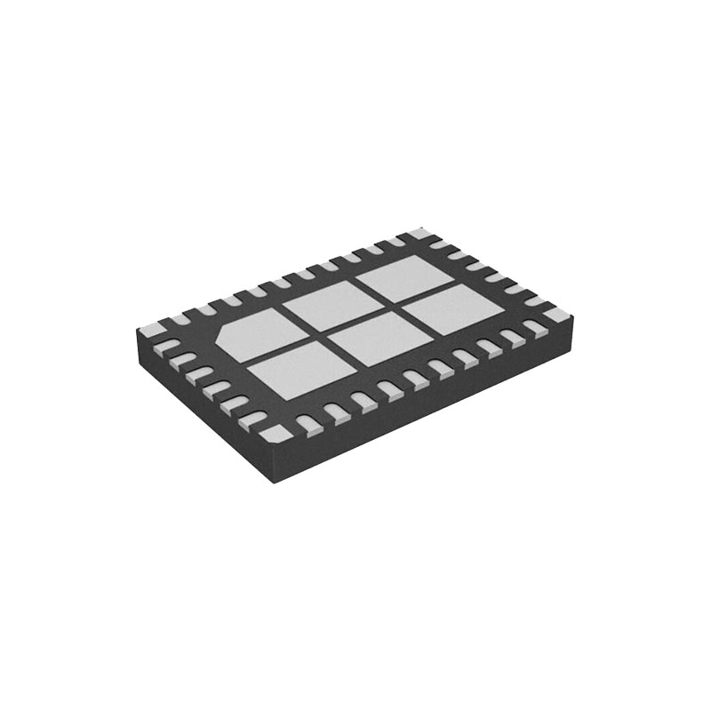
The AD9146BCPZ TxDAC+® includes features optimized for direct conversion transmit applications, including complex digital modulation, and gain and offset compensation. The DAC outputs are optimized to interface seamlessly with analog quadrature modulators, such as the ADL537x F-MOD series from Analog Devices, Inc. A 3-wire serial port interface provides for programming/readback of many internal parameters. Full-scale output current can be programmed over a range of 8.7 mA to 31.7 mA. The AD9146BCPZ comes in a 48-lead LFCSP.
A proprietary DAC output switching technique enhances dynamic performance.
The current outputs are easily configured for various single-ended or differential circuit topologies.
Compact LVDS digital interface offers reduced width data bus.
Características:
Flexible LVDS interface allows byte or nibble load
Single-carrier W-CDMA ACLR = 80 dBc at 122.88 MHz IF
Analog output: adjustable 8.7 mA to 31.7 mA,
RL = 25 Ω to 50 Ω
Integrated 2×/4× interpolator/complex modulator allows carrier placement anywhere in the DAC bandwidth
Gain, dc offset, and phase adjustment for sideband suppression
Multiple chip synchronization interfaces
High performance, low noise PLL clock multiplier
Filtro digital sinc inverso
Low power: 1.2 W @ 1.0 GSPS, 800 mW @ 500 MSPS, full operating conditions
48-lead, exposed paddle LFCSP
Aplicaciones:
Wireless infrastructure
W-CDMA, CDMA2000, TD-SCDMA, WiMAX, GSM, LTE
Digital high or low IF synthesis
Transmit diversity
Wideband communications: LMDS/MMDS, point-to-point
COMPANION PRODUCTS
IQ Modulators: ADL5370, ADL537x family
IQ Modulators with PLL and VCO: ADRF6701, ADRF670x family
Clock Drivers: AD9516, AD951x family
Voltage Regulator Design Tool: ADIsimPower
ESPECIFICACIONES
DC SPECIFICATIONS, DIGITAL SPECIFICATIONS, AC SPECIFICATIONS,
TMIN to TMAX, AVDD33 = 3.3 V, DVDD18 = 1.8 V, CVDD18 = 1.8 V, IFS = 20 mA, maximum sample rate, unless otherwise noted.
Based on a 10 kΩ external resistor between FSADJ and AVSS.
LVDS receiver is compliant with the IEEE 1596 reduced range link, unless otherwise noted.
THERMAL RESISTANCE
The exposed pad (EPAD) of the 48-lead LFCSP must be soldered to the ground plane (AVSS). The EPAD provides an electrical, thermal, and mechanical connection to the board.
Typical θJA, θJB, and θJC values are specified for a 4-layer board and an 8-layer board in still air. Airflow increases heat dissipation, effectively reducing θJA and θJB.
EPAD soldered to ground plane
TEORÍA DE FUNCIONAMIENTO
High performance, small size, and low power consumption make the AD9146 a very attractive DAC for wired and wireless communications systems. The dual digital signal path and dual DAC structure allow an easy interface to common quadrature modulators when designing single sideband (SSB) transmitters. The AD9146 offers features that allow simplified synchronization with incoming data and between multiple devices. Auxiliary DACs are also provided on chip. The auxiliary DACs can be used for output dc offset compensation (for LO compensation in SSB transmitters) and for gain matching (for image rejection optimization in SSB transmitters).
BYTE INTERFACE MODE
In byte mode, the DCI signal is a reference bit used to generate the data sampling clock and should be time aligned with the data. The most significant byte of the data should correspond to DCI high, and the least significant byte of the data should correspond to DCI low. The FRAME signal indicates to which DAC the data is sent. When FRAME is high, data is sent to the I DAC; when FRAME is low, data is sent to the Q DAC.

