DESCRIPCIÓN GENERAL
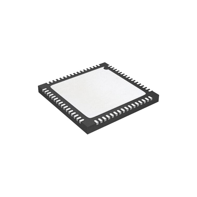
The AD9269 is a monolithic, dual-channel, 1.8 V supply, 16-bit, 20/40/65/80 MSPS analog-to-digital converter (ADC). It features a high performance sample-and-hold circuit and on-chip voltage reference. The product uses multistage differential pipeline architecture with output error correction logic to provide 16-bit accuracy at 80 MSPS data rates and to guarantee no missing codes over the full operating temperature range. The AD9269 incorporates an optional integrated dc correction and quadrature error correction block (QEC) that corrects for dc offset, gain, and phase mismatch between the two channels. This functional block can be very beneficial to complex signal processing applications such as direct conversion receivers. The ADC also contains several features designed to maximize flexibility and minimize system cost, such as programmable clock and data alignment and programmable digital test pattern AD9269 generation. The available digital test patterns include built-in deterministic and pseudorandom patterns, along with custom user-defined test patterns entered via the serial port interface (SPI). A differential clock input controls all internal conversion cycles. An optional duty cycle stabilizer (DCS) compensates for wide variations in the clock duty cycle while maintaining excellent overall ADC performance. The digital output data is presented in offset binary, gray code, or twos complement format. A data output clock (DCO) is provided for each ADC channel to ensureproper latch timing with receiving logic. Both 1.8 V and 3.3 V CMOS levels are supported, and output data can be multiplexed onto a single output bus. The AD9269 is available in a 64-lead RoHS-compliant LFCSP and is specified over the industrial temperature range (−40°C to +85°C).
PRODUCTOS DESTACADOS
1.The AD9269 operates from a single 1.8 V analog power supply and features a separate digital output driver supply to accommodate 1.8 V to 3.3 V logic families.
2.The patented sample-and-hold circuit maintains excellent performance for input frequencies up to 200 MHz and is designed for low cost, low power, and ease of use.
3.An optional SPI selectable dc correction and quadrature error correction (QEC) feature corrects for dc offset, gain, and phase mismatches between the two channels.
4.A standard serial port interface (SPI) supports various product features and functions, such as data output formatting, internal clock divider, power-down, DCO/data timing and offset adjustments, and voltage reference modes.
5.The AD9269 is packaged in a 64-lead RoHS-compliant LFCSP that is pin compatible with the AD9268 16-bit ADC, the AD9258 14-bit ADC, the AD9251 14-bit ADC the AD9231 12-bit ADC, the AD6659 12-bit baseband diversity receiver, and the AD9204 10-bit ADC, enabling a simple migration path between 10-bit and 16-bit converters sampling from 20 MSPS to 125 MSPS.
CARACTERÍSTICAS
Funcionamiento con alimentación analógica de 1,8 V
1.8 V to 3.3 V output supply
Integrated quadrature error correction (QEC)
SNR
77,6 dBFS a 9,7 MHz de entrada
71 dBFS at 200 MHz input
SFDR
93 dBc a 9,7 MHz de entrada
80 dBc at 200 MHz input
Baja potencia
44 mW per channel at 20 MSPS
100 mW per channel at 80 MSPS
Entrada diferencial con ancho de banda de 700 MHz
Referencia de tensión en chip y circuito de muestreo y retención
Entrada analógica diferencial de 2 V p-p
DNL = −0.5/+1.1 LSB
Opciones de control del puerto serie
Offset binary, gray code, or twos complement data format
Optional clock duty cycle stabilizer (DCS)
Integer 1-to-6 input clock divider
Data output multiplex option
Generación de patrones de prueba digitales seleccionables integrada
Modos de ahorro de energía
Salida de reloj de datos (DCO) con alineación programable de reloj y datos
APLICACIONES
Comunicaciones
Sistemas de radio de diversidad
Multimode digital receivers
GSM, EDGE, W-CDMA, LTE, CDMA2000, WiMAX, TD-SCDMA
I/Q demodulation systems
Sistemas de antenas inteligentes
Instrumentos a pilas
Telémetros de mano
Imagen médica portátil
Ecografía
Radar/LIDAR
TEORÍA DE FUNCIONAMIENTO
The AD9269 dual-channel ADC design can be used for diversity reception of signals, where the ADCs are operating identically on the same carrier but from two separate antennae. The ADCs can also be operated with independent analog inputs. The user can sample any fS/2 frequency segment from dc to 200 MHz, using appropriate low-pass or band-pass filtering at the ADC inputs with little loss in ADC performance. Operation to 300 MHz analog input is permitted, but it occurs at the expense of increased ADC noise and distortion. In nondiversity applications, the AD9269 can be used as a baseband or direct downconversion receiver, in which one ADC is used for I input data and the other is used for Q input data. The AD9269 incorporates an optional, integrated dc correction and quadrature error correction block (QEC) that can correct for dc offset, gain, and phase mismatch between the two channels. This functional block can be very beneficial to complex signal processing applications such as direct conversion receivers. Synchronization capability is provided to allow synchronized timing between multiple channels or multiple devices. Programming and control of the AD9269 are accomplished using a 3-wire SPI-compatible serial interface.