Descripción:
The ADP1763ACPZ is a low noise, low dropout (LDO) linear regulator. It is designed to operate from a single input supply with an input voltage as low as 1.10 V without the requirement of an external bias supply to increase efficiency and provide up to 3 A of output current.
The low 95 mV typical dropout voltage at a 3 A load allows the ADP1763ACPZ to operate with a small headroom while maintaining regulation and providing better efficiency.
The ADP1763ACPZ is optimized for stable operation with small 10 μF ceramic output capacitors. The ADP1763ACPZ delivers optimal transient performance with minimal board area.
The ADP1763ACPZ is available in fixed output voltages ranging from 0.9 V to 1.5 V. The output of the adjustable output model can be set from 0.5 V to 1.5 V through an external resistor connected between VADJ and ground.
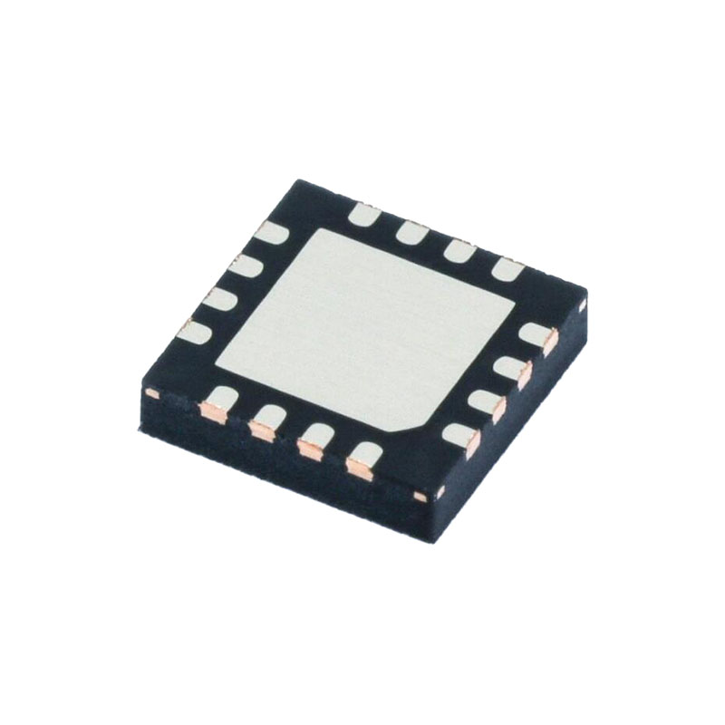
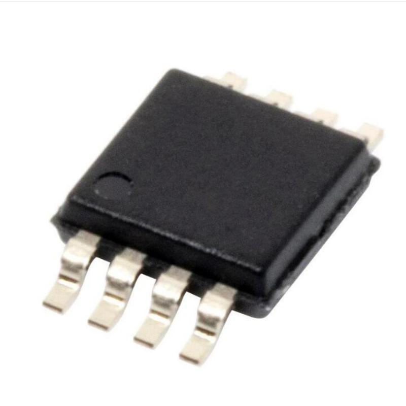
The ADP1763ACPZ has an externally programmable soft start time by connecting a capacitor to the SS pin. Short-circuit and thermal overload protection circuits prevent damage in adverse conditions. The ADP1763ACPZ is available in a small 16-lead LFCSP package for the smallest footprint solution to meet a variety of applications.
Características:
3 A maximum output current
Low input voltage supply range
VIN = 1.10 V to 1.98 V, no external bias supply required
Fixed output voltage range: VOUT_FIXED = 0.9 V to 1.5 V
Adjustable output voltage range: VOUT_ADJ = 0.5 V to 1.5 V
Ultralow noise: 2 μV rms, 100 Hz to 100 kHz
Noise spectral density
4 nV/√Hz at 10 kHz
3 nV/√Hz at 100 kHz
Low dropout voltage: 95 mV typical at 3 A load
Operating supply current: 4.5 mA typical at no load
±1.5% fixed output voltage accuracy over line, load, and temperature
Excellent power supply rejection ratio (PSRR) performance
59 dB typical at 10 kHz at 3 A load
43 dB typical at 100 kHz at 3 A load
Excellent load/line transient response
Soft start to reduce inrush current
Optimized for small 10 μF ceramic capacitors
Current-limit and thermal overload protection
Power-good indicator
Habilitación de precisión
16-lead, 3 mm × 3 mm LFCSP package
AEC-Q100 qualified for automotive applications
Aplicaciones:
Regulation to noise sensitive applications such as RF transceivers, analog-to-digital converter (ADC) and digital-to-analog converter (DAC) circuits, phase-locked loops (PLLs), voltage controlled oscillators (VCOs) and clocking integrated circuits
Field-programmable gate array (FPGA) and digital signal processor (DSP) supplies
Medicina y sanidad
Industria e instrumentación
Automoción
ESPECIFICACIONES
VIN = VOUT + 0.2 V or VIN = 1.1 V, whichever is greater, ILOAD = 10 mA, CIN = 10 µF, COUT = 10 µF, CREF = 1 µF, CREG = 1 µF, TA = 25°C, Minimum and maximum limits at TJ = −40°C to +125°C, unless otherwise noted.
1 Guaranteed by design and characterization; not production tested.
2 Based on an endpoint calculation using 10 mA and 3 A loads.
3 Dropout voltage is defined as the input to output voltage differential when the input voltage is set to the nominal output voltage, which applies only for output voltages above 1.1 V.
4 Start-up time is defined as the time from the rising edge of EN to VOUT being at 90% of its nominal value.
5 Current-limit threshold is defined as the current at which the output voltage drops to 90% of the specified typical value. For example, the current limit for a 1.0 V output voltage is defined as the current that causes the output voltage to drop to 90% of 1.0 V, or 0.9 V.
POWER-GOOD (PG) FEATURE
The ADP1763 provides a power-good pin (PG) to indicate the status of the output. This open-drain output requires an external
pull-up resistor that can be connected to VIN or VOUT. If the device is in shutdown mode, current-limit mode, or thermal shutdown, or if it falls below 90% of the nominal output voltage, PG immediately transitions low. During soft start, the rising threshold of the powergood signal is 95% of the nominal output voltage.
The open-drain output is held low when the ADP1763 has sufficient input voltage to turn on the internal PG transistor. An optional soft start delay can be detected. The PG transistor is terminated via a pull-up resistor to VOUT or VIN.
Power-good accuracy is 92.5% of the nominal regulator output voltage when this voltage is rising, with a 95% trip point when this voltage is falling.
Regulator input voltage brownouts or glitches trigger a power no good if VOUT falls below 92.5%.
A normal power-down triggers a power good when VOUT is at 95%

