DESCRIPCIÓN GENERAL
El ADP5075 es un regulador inversor de CC a CC de alto rendimiento utilizado para generar carriles de alimentación negativos. El rango de tensión de entrada de 2,85 V a 15 V admite una amplia variedad de aplicaciones. El interruptor principal integrado permite generar una tensión de salida negativa ajustable hasta 39 V por debajo de la tensión de entrada. El ADP5075 funciona a una frecuencia de conmutación de 1,2 MHz/2,4 MHz seleccionada mediante patillas. El ADP5075 puede sincronizarse con un oscilador externo de 1,0 MHz a 2,6 MHz para facilitar el filtrado de ruido en aplicaciones sensibles. El ADP5075 incluye un temporizador de arranque suave interno fijo o programable mediante resistencias para evitar la corriente de irrupción durante el encendido. Durante el apagado, el regulador desconecta completamente la carga de la alimentación de entrada para proporcionar un verdadero apagado.
CARACTERÍSTICAS
Amplio rango de tensión de entrada: de 2,85 V a 15 V
Salida negativa ajustable a VIN - 39 V
Interruptor principal integrado de 800 mA
Frecuencia de conmutación de 1,2 MHz/2,4 MHz con
sincronización de frecuencia de 1,0 MHz a 2,6 MHz
Temporizador de arranque suave programable por resistencia
Control de la velocidad de giro para reducir el ruido del sistema
Control de habilitación de precisión
Protección UVLO, OCP, OVP y TSD
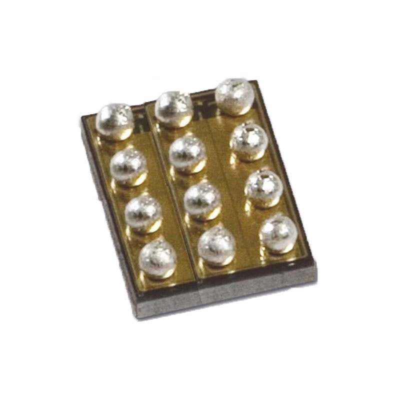
1,61 mm × 2,18 mm, WLCSP de 12 bolas
Rango de temperatura de unión de -40°C a +125°C
Compatible con el conjunto de herramientas ADIsimPower
APLICACIONES
Amplificadores bipolares, convertidores analógico-digitales (ADC),
convertidores digital-analógico (DAC) y multiplexores
Suministros de polarización para dispositivos de carga acoplada (CCD)
Suministros para módulos ópticos
Sesgo del amplificador de potencia (PA) de radiofrecuencia (RF)
MODO PWM
El regulador inversor del ADP5075 funciona a una frecuencia fija establecida por un oscilador interno. Al comienzo de cada ciclo del oscilador, el interruptor MOSFET se enciende, aplicando una tensión positiva a través del inductor. La corriente del inductor (IINDUCTOR) aumenta hasta que la señal sensora de corriente cruza el umbral de corriente pico del inductor que apaga el interruptor MOSFET; este umbral se establece mediante la salida del amplificador de error. Durante el tiempo de apagado del MOSFET, la corriente del inductor disminuye a través del diodo externo hasta que el siguiente impulso del reloj oscilador inicia un nuevo ciclo. El ADP5075 regula la tensión de salida ajustando el umbral de pico de corriente del inductor.
MODO PSM
Durante el funcionamiento con carga ligera, los reguladores pueden omitir pulsos para mantener la regulación de la tensión de salida. La omisión de impulsos aumenta la eficiencia del dispositivo.
BLOQUEO POR SUBTENSIÓN (UVLO)
El circuito de bloqueo por subtensión controla el nivel de tensión de la patilla AVIN. Si la tensión de entrada cae por debajo del umbral VUVLO_FALLING, el regulador se apaga. Cuando la tensión de la patilla AVIN supera el umbral VUVLO_RISING, se inicia el periodo de arranque suave y el regulador se activa.
REGULADORES INTERNOS
El regulador interno VREG del ADP5075 proporciona una fuente de alimentación estable para los circuitos internos. El regulador VREF proporciona una tensión de referencia para la red de realimentación del regulador inversor con el fin de garantizar una tensión de realimentación positiva en la patilla FB. Se incluye un circuito de límite de corriente para ambos reguladores internos con el fin de proteger el circuito de cargas accidentales.
PROTECCIÓN DE LÍMITE DE CORRIENTE
El regulador inversor del ADP5075 incluye circuitos de protección de límite de corriente para limitar la cantidad de corriente de avance a través del interruptor MOSFET. Cuando la corriente pico del inductor supera el umbral de límite de sobrecorriente durante un número de ciclos de reloj durante una condición de sobrecarga o cortocircuito, el regulador entra en modo de hipo. El regulador deja de conmutar y se reinicia con un nuevo ciclo de arranque suave después de tHICCUP y se repite hasta que desaparece la condición de sobrecorriente.
PROTECCIÓN CONTRA SOBRETENSIÓN
El regulador inversor dispone de un mecanismo de protección contra sobretensiones en la patilla FB. Cuando la tensión en la patilla FB cae por debajo del umbral VOV, la conmutación se detiene hasta que la tensión supera el umbral. Esta funcionalidad se activa una vez transcurrido el periodo de arranque suave.