DESCRIPCIÓN GENERAL
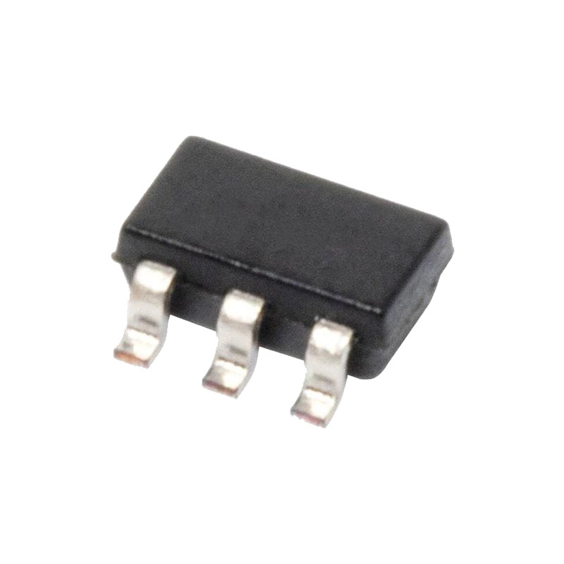
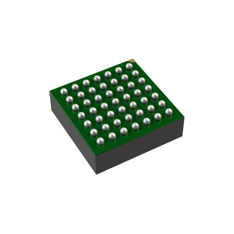
The ADP7182 is a CMOS, low dropout (LDO) linear regulator that operates from −2.7 V to −28 V and provides up to −200 mA of output current. This high input voltage LDO is ideal for regulation of high performance analog and mixed signal circuits operating from −27 V down to −1.2 V rails. Using an advanced proprietary architecture, it provides high power supply rejection and low noise, and achieves excellent line and load transient response with a small 2.2 μF ceramic output capacitor. The ADP7182 is available in fixed output voltage and an adjustable version that allows the output voltage to range from −1.22 V to −VIN + VDO via an external feedback divider. The following fixed output voltages are available from stock: −5 V (3 mm × 3 mm LFCSP), −1.8 V, −2.5 V, −3 V, −5 V (TSOT), −1.2 V, −1.5 V, −2.5 V, −5 V (2.00 mm × 2.00 mm LFCSP). Additional voltages are available by special order. The ADP7182 regulator output noise is 18 μV rms independent of the output voltage. The enable logic is capable of interfacing with positive or negative logic levels for maximum flexibility. The ADP7182 is available in 5-lead TSOT, 6- and 8-lead LFCSP packages for a small, low profile footprint.
CARACTERÍSTICAS
Low noise: 18 μV rms
Power supply rejection ratio (PSRR): 66 dB at 10 kHz at VOUT = −3 V
Positive or negative enable logic
Stable with small 2.2 μF ceramic output capacitor
Input voltage range: −2.7 V to −28 V
Maximum output current: −200 mA
Low dropout voltage: −185 mV at −200 mA load
Initial accuracy: ±1%
Accuracy over line, load, and temperature
+2% maximum/−3% minimum
Low quiescent current, IGND = −650 μA with −200 mA load
Low shutdown current: −2 μA
Adjustable output from −1.22 V to −VIN + VDO
Current-limit and thermal overload protection
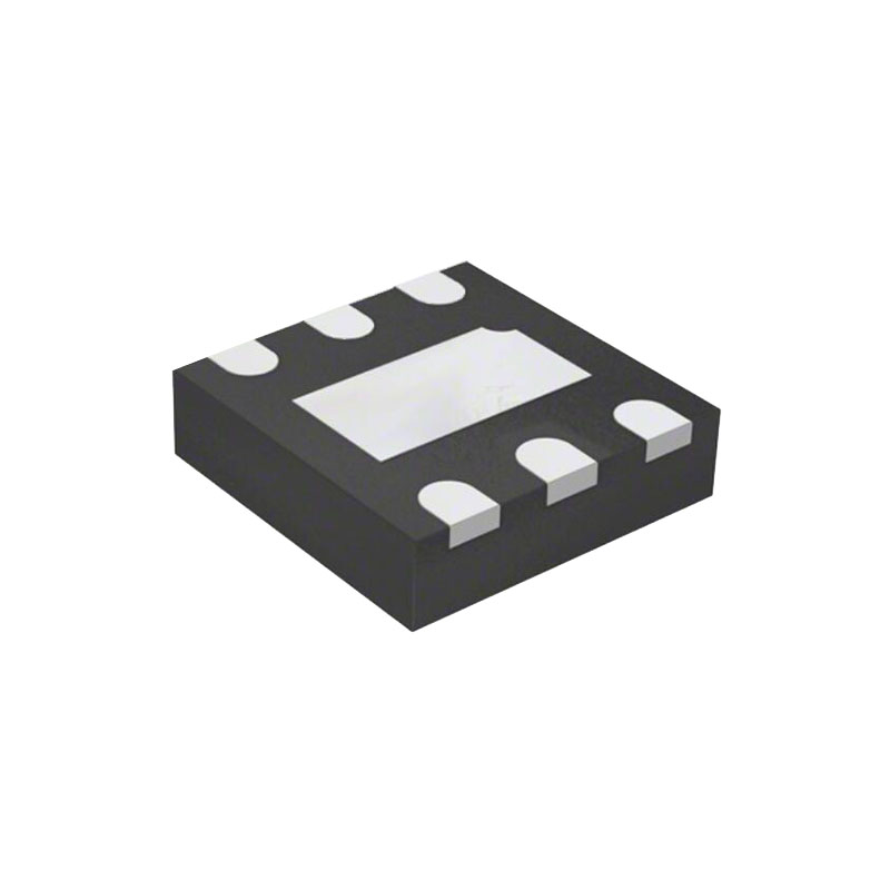
6- and 8-lead LFCSP and 5-lead TSOT
Supported by ADIsimPower tool
APLICACIONES
Regulation to noise sensitive applications
Analog-to-digital converter (ADC) and digital-to-analog
converter (DAC) circuits, precision amplifiers
Comunicaciones e infraestructuras
Medicina y sanidad
Industria e instrumentación
TEORÍA DE FUNCIONAMIENTO
The ADP7182 is a low quiescent current, LDO linear regulator that operates from −2.7 V to −28 V and can provide up to −200 mA of output current. Drawing a low −650 μA of quiescent current (typical) at full load makes the ADP7182 ideal for battery-powered portable equipment. Maximum shutdown current consumption is −8 μA at room temperature. Optimized for use with small 2.2 μF ceramic capacitors, the ADP7182 provides excellent transient performance. Internally, the ADP7182 consists of a reference, an error amplifier, a feedback voltage divider, and an NMOS pass transistor. Output current is delivered via the NMOS pass transistor, which is controlled by the error amplifier. The error amplifier compares the reference voltage with the feedback voltage from the output and amplifies the difference. If the feedback voltage is more positive than the reference voltage, the gate of the NMOS transistor is pulled toward GND, allowing more current to pass and increasing the output voltage. If the feedback voltage is more negative than the reference voltage, the gate of the NMOS transistor is pulled toward −VIN, allowing less current to pass and decreasing the output voltage. The ESD protection devices are shown in the block diagram as Zener diodes.
INFORMACIÓN SOBRE APLICACIONES
ADIsimPower DESIGN TOOL
The ADP7182 is supported by the ADIsimPower design tool set. ADIsimPower is a collection of tools that produce complete power designs optimized for a specific design goal. The tools enable the user to generate a full schematic, bill of materials, and calculate performance in minutes. ADIsimPower can optimize designs for cost, area, efficiency, and devices count taking into consideration the operating conditions and limitations of the IC and all real external components. For more information about, and to obtain ADIsimPower design tools, visit www.analog.com/ADIsimPower.

