Descripción:
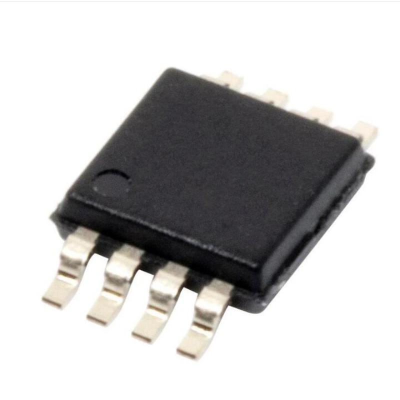
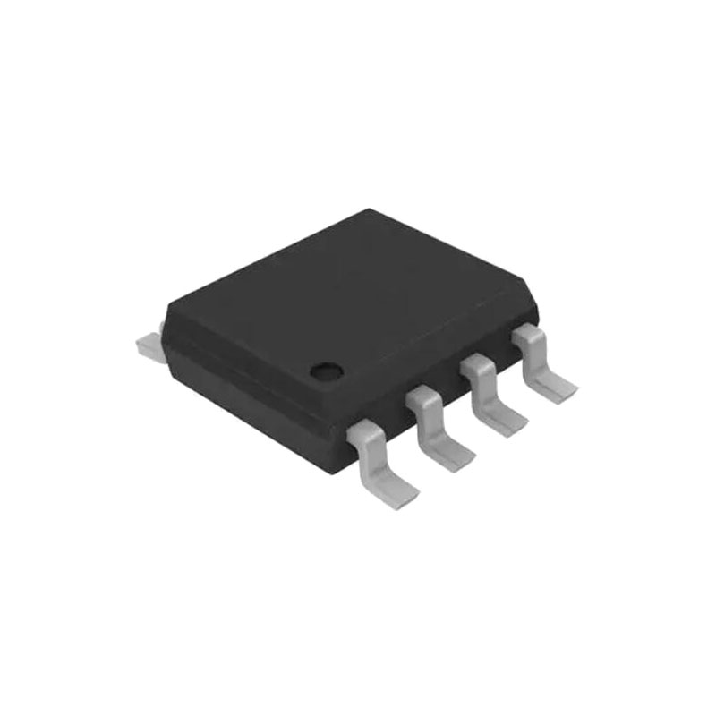
The LT1936 is a current mode PWM step-down DC/DC converter with an internal 1.9A power switch, packaged in a tiny, thermally enhanced 8-lead MSOP. The wide input range of 3.6V to 36V makes the LT1936 suitable for regulating power from a wide variety of sources, including automotive batteries, 24V industrial supplies and unregulated wall adapters. Its high operating frequency allows the use of small, low cost inductors and ceramic capacitors, resulting in low, predictable output ripple.
Cycle-by-cycle current limit, frequency foldback and thermal shutdown provide protection against shorted outputs, and soft-start eliminates input current surge during startup. Transient response can be optimized by using external compensation components, or board space can be minimized by using internal compensation. The low current (<2µA) shutdown mode enables easy power management in battery-powered systems.
Características:
Amplio rango de entrada: 3,6 V a 36 V
Short-Circuit Protected Over Full Input Range
1.9A Guaranteed Minimum Switch Current
5V at 1.4A from 10V to 36V Input
3.3V at 1.4A from 7V to 36V Input
5V at 1.2A from 6.3V to 36V Input
3.3V at 1.2A from 4.5V to 36V Input
Output Adjustable Down to 1.20V
500kHz Fixed Frequency Operation
Arranque suave
Uses Small Ceramic Capacitors
Internal or External Compensation
Low Shutdown Current: <2µA
Aplicaciones:
Regulación de baterías de automoción
Suministros de control industrial
Unregulated Wall Adapters
CARACTERÍSTICAS ELÉCTRICAS
The denotes the specifi cations which apply over the full operating temperature range, otherwise specifi cations are at TA = 25°C. VIN = 12V, VBOOST = 17V, unless otherwise noted.
Nota 1: Las tensiones superiores a las indicadas en los valores nominales máximos absolutos pueden provocar daños permanentes en el dispositivo. La exposición a cualquier condición de máxima tensión absoluta durante periodos prolongados puede afectar a la fiabilidad y la vida útil del dispositivo.
Note 2: The LT1936E is guaranteed to meet performance specifi cations from 0°C to 70°C. Specifi cations over the –40°C to 85°C operating temperature range are assured by design, characterization and correlationwith statistical process controls. The LT1936I specifi cations are guaranteed over the –40°C to 125°C temperature range. The LT1936H specifi cations are guaranteed over the –40°C to 150°C temperature range.
Note 3: Current limit guaranteed by design and/or correlation to static test. Slope compensation reduces current limit at higher duty cycle.
Note 4: Current fl ows out of pin.
Note 5: Current fl ows into pin.
FUNCIONES DEL PIN
BOOST (Pin 1): The BOOST pin is used to provide a drive voltage, higher than the input voltage, to the internal bipolar NPN power switch.
VIN (Pin 2): The VIN pin supplies current to the LT1936’s internal regulator and to the internal power switch. This pin must be locally bypassed.
SW (Pin 3): The SW pin is the output of the internal power switch. Connect this pin to the inductor, catch diode and boost capacitor.
GND (Pin 4): Tie the GND pin to a local ground plane below the LT1936 and the circuit components. Return the feedback divider to this pin.
SHDN (Pin 5): The SHDN pin is used to put the LT1936 in shutdown mode. Tie to ground to shut down the LT1936. Tie to 2.3V or more for normal operation. If the shutdown feature is not used, tie this pin to the VIN pin. SHDN also provides a soft-start function; see the Applications Information. Do not drive SHDN more than 5V above VIN.
FB (Pin 6): The LT1936 regulates its feedback pin to 1.200V. Connect the feedback resistor divider tap to this pin. Set the output voltage according to VOUT = 1.200V (1 + R1/R2). A good value for R2 is 10k.
VC (Pin 7): The VC pin is used to compensate the LT1936 control loop by tying an external RC network from this pin to ground. The COMP pin provides access to an internal RC network that can be used instead of the external components.
COMP (Pin 8): To use the internal compensation network, tie the COMP pin to the VC pin. Otherwise, tie COMP to ground or leave it fl oating.
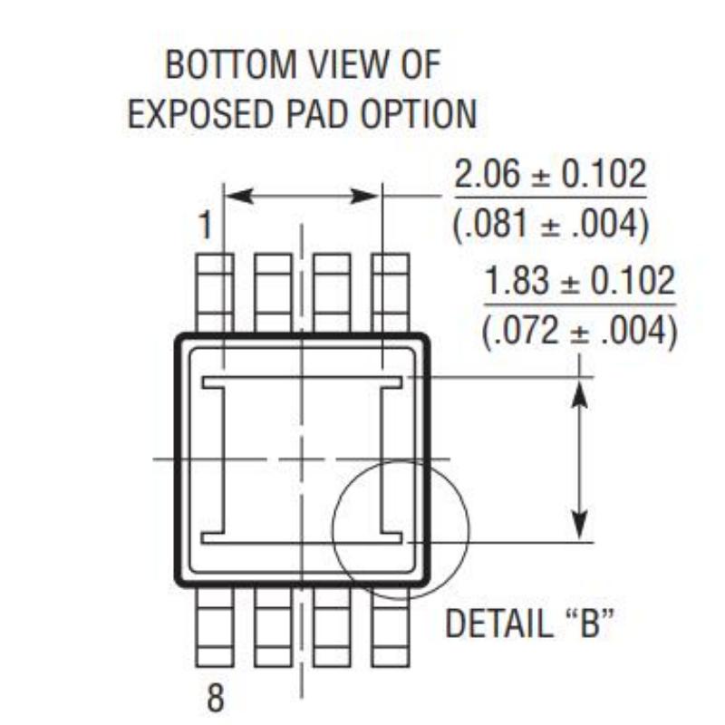
Exposed Pad (Pin 9): The Exposed Pad must be soldered to the PCB and electrically connected to ground. Use a large ground plane and thermal vias to optimize thermal performance.

