DESCRIPCIÓN
El LT3042 es un regulador lineal de alto rendimiento y baja caída que incorpora la arquitectura de ruido ultrabajo y PSRR ultraalta de LTC para alimentar aplicaciones de RF sensibles al ruido. Diseñado como una referencia de corriente de precisión seguida de un búfer de tensión de alto rendimiento, el LT3042 se puede poner fácilmente en paralelo para reducir aún más el ruido, aumentar la corriente de salida y distribuir el calor en la placa de circuito impreso.
El dispositivo suministra 200 mA a una tensión de desconexión típica de 350 mV. La corriente de reposo de funcionamiento es nominalmente de 2 mA y desciende a <<1μA en apagado. El amplio rango de tensión de salida del LT3042 (0V a 15V), manteniendo un funcionamiento de ganancia unitaria, proporciona un ruido de salida, PSRR, ancho de banda y regulación de carga prácticamente constantes, independientemente de la tensión de salida programada. Además, el regulador dispone de límite de corriente programable, capacidad de arranque rápido y potencia buena programable para indicar la regulación de la tensión de salida.
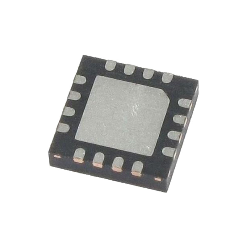
El LT3042 es estable con un condensador de salida cerámico mínimo de 4,7μF. La protección incorporada incluye protección de batería inversa, protección de corriente inversa, límite de corriente interno con retroceso y límite térmico con histéresis. El LT3042 está disponible en encapsulados MSOP de 10 terminales y DFN de 3 mm × 3 mm térmicamente mejorados.
CARACTERÍSTICAS
Ruido RMS ultrabajo: 0,8μVRMS (10 Hz a 100 kHz)
Ruido puntual ultrabajo: 2nV/√Hz a 10kHz
PSRR ultraalta: 79 dB a 1 MHz
Corriente de salida: 200 mA
Amplio rango de tensión de entrada: 1,8 V a 20 V
Un único condensador mejora el ruido y la PSRR
100μA Corriente del pin SET: ±1% Precisión inicial
Programas de una sola resistencia Tensión de salida
Gran ancho de banda: 1 MHz
Límite de corriente programable
Baja tensión de caída: 350 mV
Rango de tensión de salida: 0V a 15V
Buena potencia programable
Rápida puesta en marcha
Habilitación de precisión/UVLO
Conectable en paralelo para reducir el ruido y aumentar la corriente
Límite de corriente interno con Foldback
Condensador de salida mínimo: 4,7μF cerámico
Protección de batería inversa y corriente inversa
MSOP de 10 terminales y DFN de 3 mm × 3 mm
Cualificación AEC-Q100 para aplicaciones de automoción
APLICACIONES
Fuentes de alimentación RF: PLLs, VCOs, Mezcladores, LNAs
Instrumentación de muy bajo ruido
Convertidores de datos de alta velocidad y precisión
Aplicaciones médicas: Imagen, diagnóstico
Fuentes de alimentación de precisión
Postregulador para fuentes de alimentación conmutadas
INFORMACIÓN SOBRE APLICACIONES
El LT3042 es un regulador lineal de bajo dropout y alto rendimiento que presenta la arquitectura de ruido ultrabajo (2nV/√Hz a 10kHz) y PSRR ultra alta (79dB a 1MHz) de LTC para alimentar aplicaciones sensibles al ruido. Diseñado como una fuente de corriente de precisión seguida de un búfer de tensión de carril a carril de alto rendimiento, el LT3042 puede ponerse fácilmente en paralelo para reducir aún más el ruido, aumentar la corriente de salida y repartir el calor en la placa de circuito impreso. El dispositivo cuenta además con límite de corriente programable, capacidad de arranque rápido y buena potencia programable. El LT3042 es fácil de usar e incorpora todas las características de protección que se esperan de los reguladores de alto rendimiento. Incluye protección contra cortocircuitos, protección de zona de funcionamiento seguro, protección de batería inversa, protección de corriente inversa y desconexión térmica con histéresis.
Funciones de protección
El LT3042 incorpora varias funciones de protección para aplicaciones alimentadas por batería. El límite de corriente de precisión y la protección contra sobrecarga térmica protegen al LT3042 contra condiciones de sobrecarga y fallo en la salida del dispositivo. Para un funcionamiento normal, no permita que la temperatura de unión supere los 125°C (grado E, I) o los 150°C (grado H, MP).
Para proteger el amplificador de error de bajo ruido del LT3042, la pinza de protección SETto- OUTS limita la tensión máxima entre SET y OUTS con una corriente continua máxima de 20mA a través de la pinza. Por lo tanto, para aplicaciones en las que SET es controlado activamente por una fuente de tensión, la fuente de tensión debe limitarse a 20 mA o menos. Además, para limitar la corriente transitoria que fluye a través de estas pinzas durante una condición de fallo transitorio, limite el valor máximo del condensador de la patilla SET (CSET) a 22μF.
El LT3042 también incorpora protección de entrada inversa mediante la cual el pin IN soporta tensiones inversas de hasta -20V sin causar ningún flujo de corriente de entrada y sin desarrollar tensiones negativas en el pin OUT. El regulador se protege a sí mismo y a la carga contra las baterías que se conectan al revés.
En los circuitos en los que se requiere una batería de reserva, pueden darse varias condiciones de entrada/salida diferentes. La tensión de salida puede mantenerse mientras la entrada se lleva a GND, a una tensión intermedia o se deja en circuito abierto. En todos estos casos, el circuito de protección de corriente inversa impide el flujo de corriente desde la salida a la entrada. No obstante, debido a la pinza OUTS-to-SET, a menos que la patilla SET esté flotando, la corriente puede fluir a GND a través de la resistencia de la patilla SET, así como hasta 15 mA a GND a través del circuito de recuperación del sobreimpulso de salida. Este flujo de corriente a través del circuito de recuperación de sobreimpulso de salida puede reducirse significativamente colocando un diodo Schottky entre las patillas OUTS y SET, con su ánodo en la patilla OUTS.