CARACTERÍSTICAS
Interruptor de alimentación interno de 2 A
Frecuencia de conmutación ajustable
Una sola resistencia de realimentación ajusta VOUT
Sincronizable con reloj externo
La clavija SHDN de alta ganancia acepta señales de entrada que varían lentamente
Amplio rango de tensión de entrada: de 2,5 V a 32 V
Interruptor VCESAT bajo: 300 mV a 1,5 A (típico)
Función de arranque suave integrada
Fácilmente configurable como convertidor Boost o inversor
Bloqueo por subtensión (UVLO) configurable por el usuario
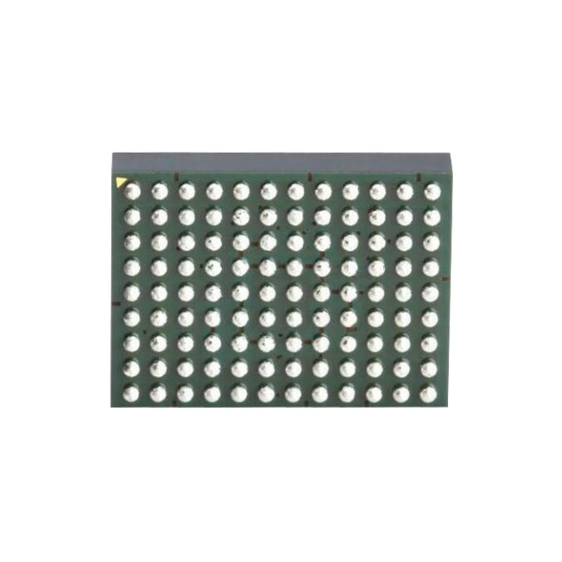
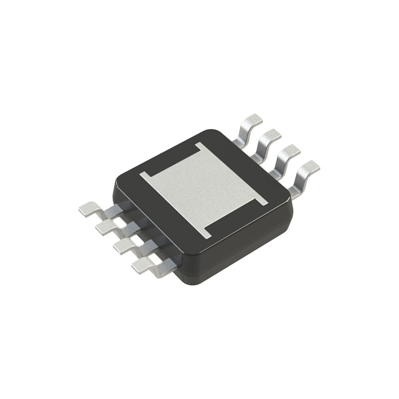
Encapsulados DFN y MSOP diminutos de 8 conductores y 3 mm × 3 mm
APLICACIONES
Suministros de polarización VFD
Suministros de polarización TFT-LCD
Receptores GPS
Módems DSL
Fuente de alimentación local
DESCRIPCIÓN
El LT®3580 es un convertidor DC/DC PWM que contiene un interruptor interno de 2A, 42V. El LT3580 puede configurarse como un convertidor boost, SEPIC o inversor. Capaz de generar 12V a 550mA o -12V a 350mA a partir de una entrada de 5V, el LT3580 es ideal para muchos diseños de fuentes de alimentación locales.
El LT3580 tiene un oscilador ajustable, fijado por una resistencia del pin RT a masa. Además, el LT3580 puede sincronizarse con un reloj externo. El rango de frecuencia de conmutación libre o sincronizada de la pieza se puede ajustar entre 200 kHz y 2,5 MHz.
El LT3580 también incorpora un innovador circuito de patillas SHDN que permite señales de entrada de variación lenta y una función de bloqueo por subtensión ajustable.
Incorpora funciones adicionales, como el repliegue de frecuencia y el arranque suave. El LT3580 está disponible en encapsulados DFN de 3 mm × 3 mm y MSOP de 8 terminales.
OPERACIÓN
El LT3580 utiliza un esquema de control en modo de corriente y frecuencia constante para proporcionar una excelente regulación de línea y carga. Consulte el diagrama de bloques que muestra el LT3580 en una configuración boost. Al comienzo de cada ciclo del oscilador, el SR latch (SR1) se activa, lo que enciende el interruptor de potencia, Q1. La corriente del interruptor fluye a través de la resistencia sensora de corriente interna generando un voltaje proporcional a la corriente del interruptor. Esta tensión (amplificada por A4) se añade a una rampa de estabilización y la suma resultante se introduce en el terminal positivo del comparador PWM A3. Cuando esta tensión supera el nivel en la entrada negativa de A3, el SR latch se resetea, apagando el interruptor de potencia. El nivel en la entrada negativa de A3 (pin VC) es fijado por el amplificador de error A1 (o A2) y es simplemente una versión amplificada de la diferencia entre la tensión de realimentación (pin FB) y la tensión de referencia (1.215V o 5mV dependiendo de la configuración). De esta forma, el amplificador de error establece el nivel de corriente de pico correcto para mantener la salida en regulación.
El LT3580 tiene una novedosa arquitectura de patillas FB que puede utilizarse para configuraciones de refuerzo o de inversión. Cuando se configura como convertidor elevador, la patilla FB se eleva a la tensión de polarización interna de 1,215 V mediante la resistencia RFB conectada de VOUT a FB. El comparador A2 queda inactivo y el comparador A1 realiza la amplificación inversora de FB a VC. Cuando el LT3580 está en una configuración inversa, el pin FB es bajado a 5mV por la resistencia RFB conectada desde VOUT a FB. El comparador A1 se inactiva y el comparador A2 realiza la amplificación no inversora de FB a VC.
Topología SEPIC
El LT3580 puede configurarse como un SEPIC (convertidor de inductancia primaria de un solo extremo). Esta topología permite que la entrada sea mayor, igual o menor que la tensión de salida deseada. La desconexión de salida está inherentemente incorporada en la topología SEPIC, lo que significa que no existe ningún camino de CC entre la entrada y la salida. Esto es útil para aplicaciones que requieren que la salida se desconecte de la fuente de entrada cuando el circuito está apagado.
Topología inversa
El LT3580 también puede funcionar en una topología inversora de doble inductor. El exclusivo pin de realimentación de la pieza permite construir la topología inversora simplemente cambiando la conexión de los componentes externos. Esta solución da como resultado un rizado de tensión de salida muy bajo debido al inductor L2 en serie con la salida. Los cambios bruscos en la corriente del condensador de salida se eliminan porque el inductor de salida suministra corriente a la salida tanto durante el tiempo de apagado como durante el tiempo de encendido del interruptor LT3580.