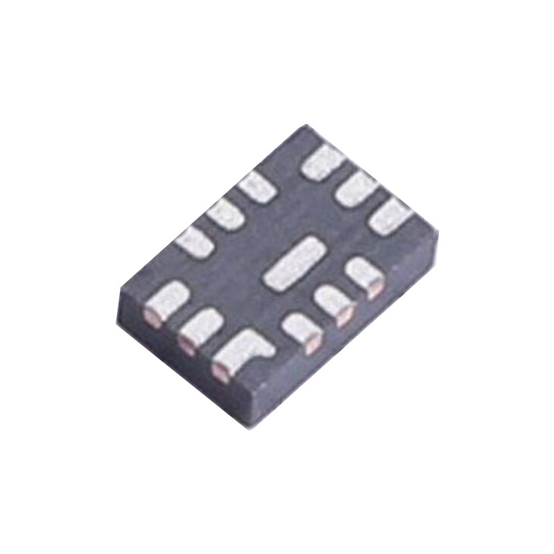
DESCRIPTION GÉNÉRALE
L'ADATE207 est un générateur de temps et un formateur pour les équipements de test automatique (ATE). L'ADATE207 fournit quatre canaux indépendants avec un taux de vecteur de base de 100 MHz de synchronisation et de formatage pour les broches numériques ATE. Il assure l'interface entre la mémoire de motifs et les puces de pilotage, de comparaison et de charge (DCL) pour les broches numériques complètes. L'ADATE207 accepte jusqu'à huit bits de données de modèle par broche et peut produire des sorties formatées et effectuer des comparaisons des réponses attendues de l'objet sous test.
Chaque canal de l'ADATE207 fournit 256 formes d'onde sélectionnables, chaque forme d'onde comprenant jusqu'à quatre événements possibles. Chaque événement consiste en un front de synchronisation programmable et un ensemble compatible STIL (IEEE Standard 1450-1999).
Chaque générateur d'arête de synchronisation peut produire une arête avec une portée de quatre périodes avec une résolution de placement d'arête de 39,06 ps. Les générateurs de retard utilisent une horloge maître de référence de 100 MHz et fournissent des retards programmables basés sur les comptes de l'horloge et un vernier de synchronisation analogique CMOS compensé. Les générateurs de retard programmables peuvent être retardés en plus par une valeur d'entrée globale de 8 bits qui est partagée sur tous les fronts.
Le format et la logique de comparaison prennent en charge le multiplexage de broches ×2 pour permettre l'échange du nombre de broches contre la vitesse.
Chaque canal fournit une capture de sortie de l'objet à tester de 4 bits, prenant en charge les applications de mémoire de réception à signaux mixtes. La logique de détection des défaillances comprend un registre d'accumulation des défaillances de 32 bits par canal.
Un TMU externe est pris en charge avec trois multiplexeurs 8 à 1. Cela permet de multiplexer les sorties du double comparateur de n'importe quelle broche vers n'importe laquelle des trois sorties : signaux d'armement, de démarrage ou d'arrêt.
CARACTÉRISTIQUES
Formateur de temps à 4 canaux
256 formes d'onde par canal
4 fronts d'événements indépendants par forme d'onde
STIL Événements compatibles avec la norme IEEE 1450-1999
Gamme de 4 périodes pour chaque bord
39,06 ps résolution temporelle
2,5 ns taux de réactivation du front minimal
Tous les formats de lecteur sont pris en charge
Taux vectoriel de base de 100 MHz ×2 et ×4 modes haute vitesse ×2 broches de multiplexage
Largeur d'impulsion minimale de 1 ns Compteur de défaillances 32 bits par canal
Capture de broches sur 4 bits par canal
Refroidissement par air, conception CMOS à faible consommation
6 W à une fréquence de base de 100 MHz
Alimentation 2,5 V
Contrôle de l'interface DCL différentielle
Multiplexeur TMU
CANDIDATURES
Équipement de test automatique (ATE) Instrumentation numérique à grande vitesse Génération d'impulsions
THÉORIE DU FONCTIONNEMENT
MÉMOIRE DE FORME D'ONDE
Les données de modèle sont utilisées pour adresser la mémoire de forme d'onde et ont une largeur de huit bits par canal, ce qui permet de prendre en charge 256 formes d'onde uniques. La largeur des données de la mémoire de forme d'onde est de 26 bits par événement ou de 104 bits par broche. Les bits de données de la mémoire de forme d'onde sont divisés en deux champs, un champ de retard de 22 bits de large et un champ de code d'événement de 4 bits. La mémoire de forme d'onde est à double port, ce qui permet à l'unité centrale d'y accéder pendant l'éclatement du motif. Les données de modèle sont utilisées comme pointeur vers l'une des 256 formes d'onde définies et peuvent être divisées en données vectorielles et en pointeur d'ensemble de temps. En utilisant trois bits de données vectorielles pour l'état de la broche, les cinq autres bits peuvent être utilisés comme 32 ensembles de temps possibles. Dans le cas d'une double E/S par cycle, deux ensembles de données vectorielles de 3 bits peuvent être utilisés en combinaison avec deux bits d'un pointeur d'ensemble de temps, ce qui donne quatre
les ensembles de temps possibles. Il est possible de faire un compromis direct entre les ensembles de temps et les vecteurs de dispositif par cycle de test. Les données du modèle sont qualifiées par le signal d'entrée PAT_DATA_VALID. Lorsqu'il est activé, les données du modèle sont évaluées. S'il n'est pas activé, les événements et les fronts de synchronisation sont désactivés et les données du modèle d'entrée sont ignorées.
GÉNÉRATEURS D'ÉVÉNEMENTS
Chaque canal dispose de quatre générateurs d'événements programmables. Chaque générateur d'événements entre un délai, un code d'événement provenant de la mémoire de forme d'onde et un INPUT_DELAY de 8 bits. Le retard de la forme d'onde et le délai d'entrée de 8 bits se combinent pour produire des retards programmables à partir des démarrages de cycles T0. Chaque retard programmable peut couvrir jusqu'à 4 périodes T0 et jusqu'à 163 μs avec une résolution de retard nominale de 39,06 ps. Il existe 16 événements possibles. Ces événements sont les suivants
compatible avec les événements de forme d'onde STIL, comme indiqué dans le tableau 8, pour créer tous les formats conventionnels d'entraînement et de comparaison. Il existe un délai programmable avec une résolution de 2,5 ns entre les événements d'entraînement et les événements de comparaison, ce qui permet de compenser le délai d'aller-retour (RTD).