DESCRIPTION GÉNÉRALE
The AD8421 is a low cost, low power, extremely low noise, ultralow bias current, high speed instrumentation amplifier that is ideally suited for a broad spectrum of signal conditioning and data acquisition applications. This product features extremely high CMRR, allowing it to extract low level signals in the presence of high frequency common-mode noise over a wide temperature range.
The 10 MHz bandwidth, 35 V/μs slew rate, and 0.6 μs settling time to 0.001% (G = 10) allow the AD8421 to amplify high speed signals and excel in applications that require high channel count, multiplexed systems. Even at higher gains, the current feedback architecture maintains high performance; for example, at G = 100, the bandwidth is 2 MHz and the settling time is 0.8 μs. The AD8421 has excellent distortion performance, making it suitable for use in demanding applications such as vibration analysis.
The AD8421 delivers 3 nV/√Hz input voltage noise and 200 fA/√Hz current noise with only 2 mA quiescent current, making it an ideal choice for measuring low level signals. For applications with high source impedance, the AD8421 employs innovative process technology and design techniques to provide noise performance that is limited only by the sensor.
The AD8421 uses unique protection methods to ensure robust inputs while still maintaining very low noise. This protection allows input voltages up to 40 V from the opposite supply rail without damage to the part.
A single resistor sets the gain from 1 to 10,000. The reference pin can be used to apply a precise offset to the output voltage.
The AD8421 is specified from −40°C to +85°C for the 8-lead MSOP and SOIC packages, and from −40°C to +125°C for the 8-lead LFCSP package.
CARACTÉRISTIQUES
Faible consommation
2.3 mA maximum supply current
Low noise
3.2 nV/√Hz maximum input voltage noise at 1 kHz
200 fA/√Hz current noise at 1 kHz
Excellent ac specifications
10 MHz bandwidth (G = 1)
2 MHz bandwidth (G = 100)
80 dB CMRR at 20 kHz (G = 1)
35 V/μs slew rate
High precision dc performance (AD8421BRZ)
94 dB CMRR minimum (G = 1)
0.2 μV/°C maximum input offset voltage drift
1 ppm/°C maximum gain drift (G = 1)
500 pA maximum input bias current
Inputs protected to 40 V from opposite supply
±2.5 V to ±18 V dual supply (5 V to 36 V single supply)
Gain set with a single resistor (G = 1 to 10,000)
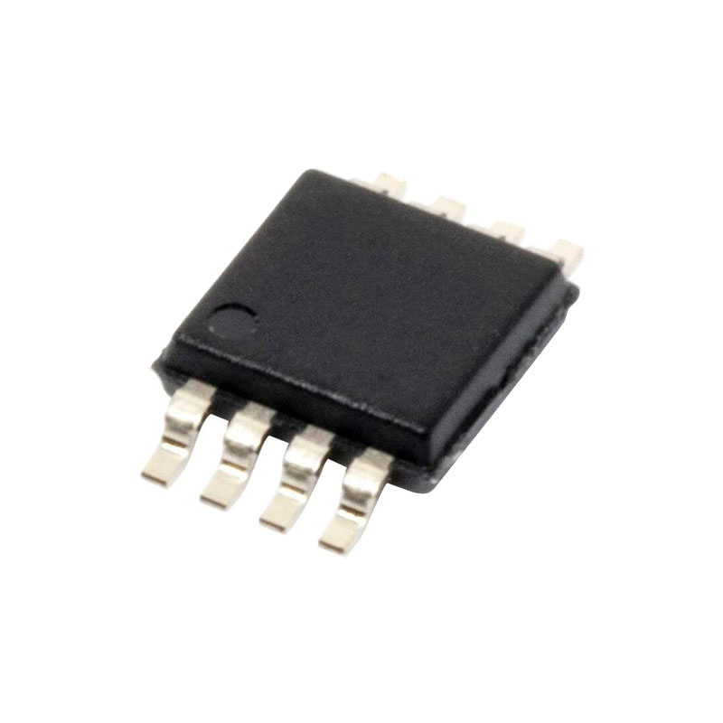
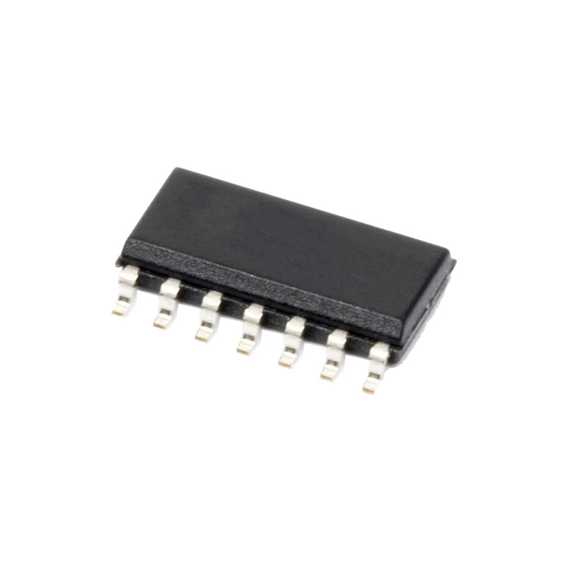
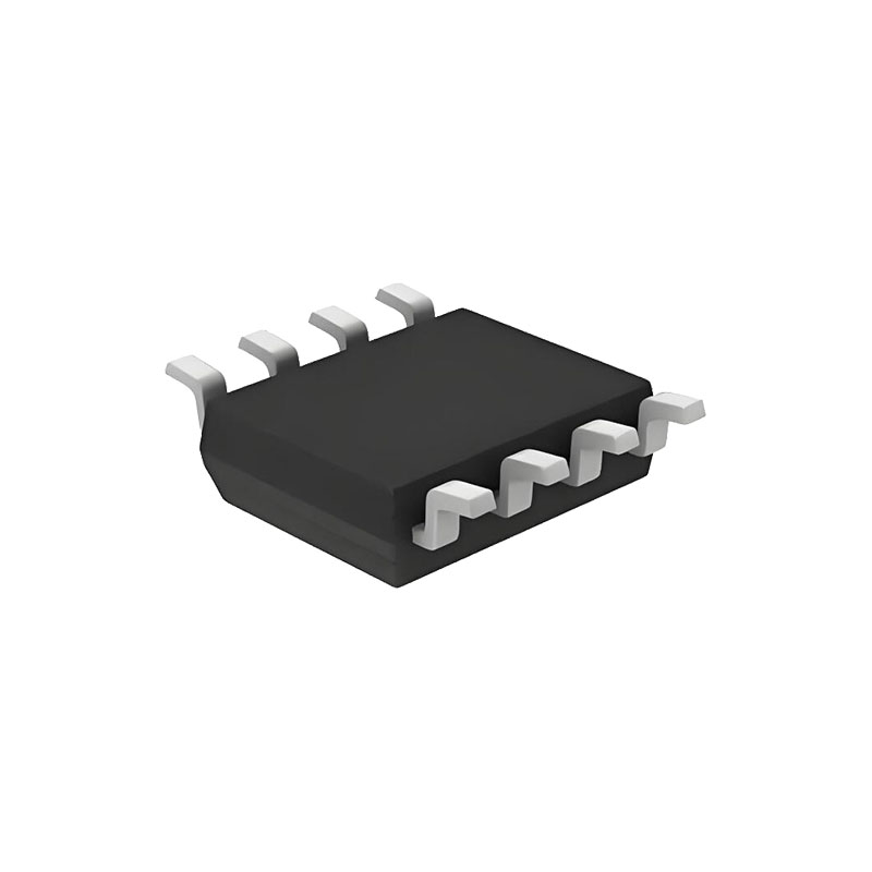
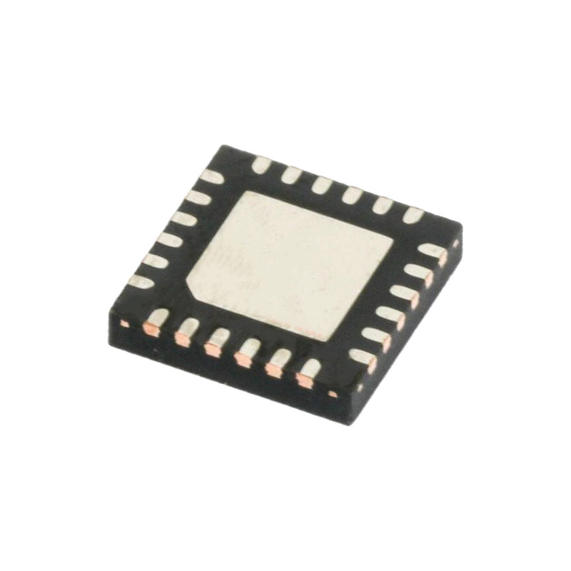
Available in 8-lead LFCSP, 8-lead MSOP, and 8-lead SOIC
CANDIDATURES
Instruments médicaux
Precision data acquisition
Microphone preamplification
Vibration analysis
Multiplexed input applications
Pilote ADC
THÉORIE DU FONCTIONNEMENT
ARCHITECTURE
The AD8421 is based on the classic 3-op-amp topology. This topology has two stages: a preamplifier to provide differential amplification, followed by a difference amplifier that removes the common-mode voltage.
Topologically, Q1, A1, R1 and Q2, A2, R2 can be viewed as precision current feedback amplifiers. Input Transistors Q1 and Q2 are biased at a fixed current so that any input signal forces the output voltages of A1 and A2 to change accordingly. The differential signal applied to the inputs is replicated across the RG pins. Any current through RG also flows through R1 and R2, creating a gained differential voltage between Node 1 and Node 2.
The amplified differential and common-mode signals are applied to a difference amplifier that rejects the common-mode voltage but preserves the amplified differential voltage. The difference amplifier employs innovations that result in very low output errors such as offset voltage and drift, distortion at various loads, as well as output noise. Laser-trimmed resistors allow for a highly accurate in-amp with gain error less than 0.01% and CMRR that exceeds 94 dB (G = 1). The high performance pinout and special attention given to design and layout allow for high CMRR performance across a wide frequency and temperature range.
Using superbeta input transistors and bias current compensation, the AD8421 offers extremely high input impedance, low bias cur-rent, low offset current, low current noise, and extremely low voltage noise of 3 nV/√Hz. The current-limiting and overvoltage protection scheme allow the input to go 40 V from the opposite rail at all gains without compromising the noise performance.
Users can easily and accurately set the gain using a single standard resistor.

