DESCRIPTION
The LT3582/LT3582-5/LT3582-12 are dual DC/DC converters featuring positive and negative outputs and integrated feedback resistors. The LT3582, with its built-in One Time Programming (OTP), has confi gurable output settings via the I2C interface, including output voltage settings, power-up sequencing, power-down discharge, and output voltage ramp rates. LT3582 settings can be changed adaptively in the fi nal product, or set during manufacturing and made permanent using the built in non-volatile OTP memory. The positive output voltage can be set between 3.2V and 12.775V in 25mV steps. The negative output voltage can be set between -1.2V and –13.95V in –50mV steps. The LT3582-5 and LT3582-12 are pre-confi gured at the factory for ±5V and ±12V outputs respectively, and as such, don’t require the use of the I2C interface.
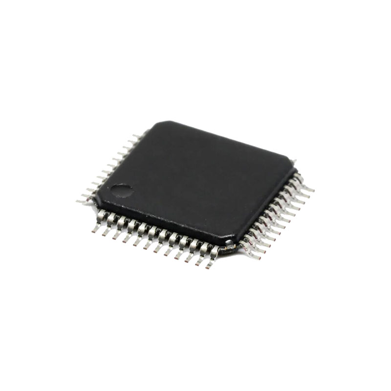
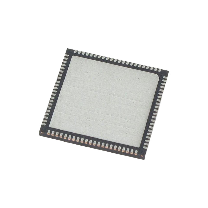
The LT3582 series includes two monolithic converters, one Boost and one Inverting. The Boost converter has an integrated power switch and output disconnect switch. The Inverting converter uses a single inductor topology and includes an integrated power switch. Both Boost and Inverting converters use a novel** control scheme resulting in low output voltage ripple while allowing for high conversion effi ciency over a wide load current range. The LT3582 series is available in a 16-pin 3mm × 3mm QFN.
CARACTÉRISTIQUES
Output Voltages:
3.2V to 12.775V and –1.2V to –13.95V (LT3582)
5V and –5V (LT3582-5)
12V and –12V (LT3582-12)
Digitally Re-Programmable (LT3582) via I2C for:
Output Voltages
Power Sequencing
Output Voltage Ramp Rates
Power-Up Defaults Settable with Non-Volatile OTP (LT3582)
I2C Compatible Interface (Standard Mode*)
All Power Switches Integrated
350mA Current Limit (Boost)
600mA Current Limit (Inverting)
All Feedback Resistors Integrated
Input Voltage Range: 2.55V to 5.5V
Faible courant de repos
325μA in Active Mode
0.01μA in Shutdown Mode
Integrated Output Disconnect
Tiny 16-Pin 3mm × 3mm QFN Package
CANDIDATURES
AMOLED Power
CCD Power
General Purpose DC/DC Conversion
FONCTIONNEMENT
The LT3582 series are dual DC/DC converters, each containing both a Boost and an Inverting converter. Operation can be best understood by referring to the Block Diagram. The Boost and Inverting converters each use a novel control technique, which simultaneously varies both peak inductor current and switch off time. This results in high effi ciency over a large load range and low output voltage ripple. In addition, this technique further minimizes output ripple when the switching frequency is in the audio band.
Boost Converter: The Boost converter uses a grounded source NMOS power transistor as the main switching element. The current in the NMOS is constantly monitored and controlled, along with the off-time of the switch to achieve regulation of VOUTP. The VOUTP voltage is divided by the internal programmable (LT3582 only) resistor divider to create FBP. The voltage on FBP is compared to an internal reference and amplifi ed, creating an error signal on the VCP node which commands the appropriate peak inductor current and off time for the subsequent switching cycle.
Output Power-Up Sequencing: After an initial start-up delay (TSTART-UP = 64μs typical), the outputs VOUTP and VOUTN rise (in magnitude) simultaneously with the LT3582-5/ LT3582-12 or in one of four selectable sequences with the LT3582. Using the I2C interface, the LT3582 outputs can be configured such that (1) they both rise simultaneously, (2) VOUTP rises to regulation before VOUTN rises, (3) VOUTN rises to regulation before VOUTP rises, or (4) neither output rises. The outputs of the LT3582-5 and LT3582-12 are pre-confi gured to rise simultaneously.
The ramp rates of the outputs are proportional to the ramp rates of their respective RAMP pins. A capacitor is placed between each RAMP pin and ground. The RAMP pins are discharged during shutdown. Once enabled, confi gurable (LT3582) or pre-confi gured (LT3582-5/LT3582-12) currents charge each RAMP pin in the desired sequence causing the outputs to rise.