Description :
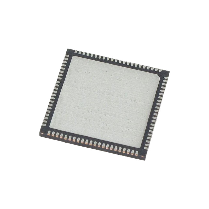
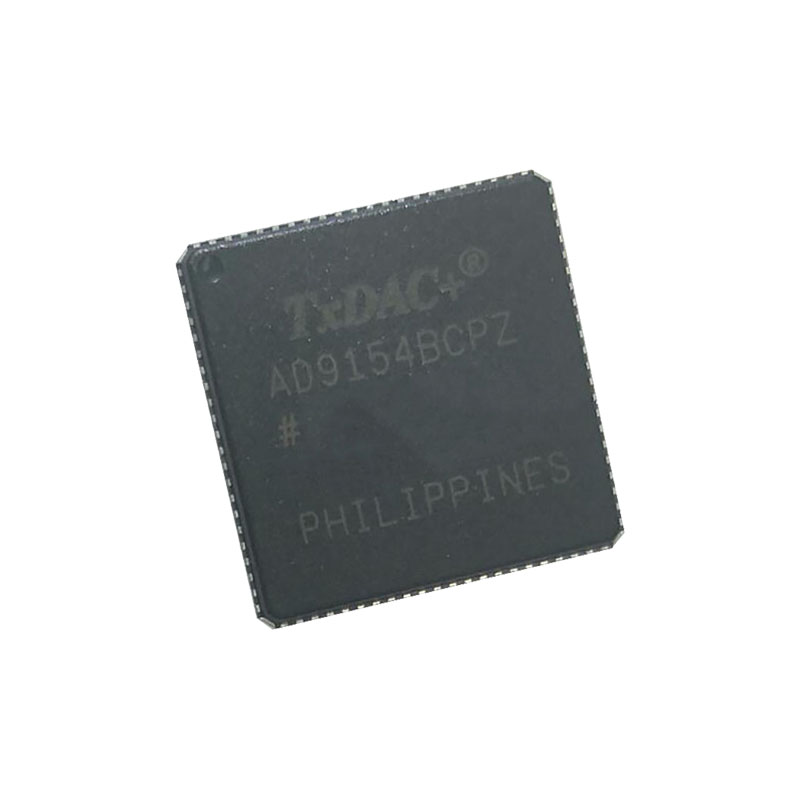
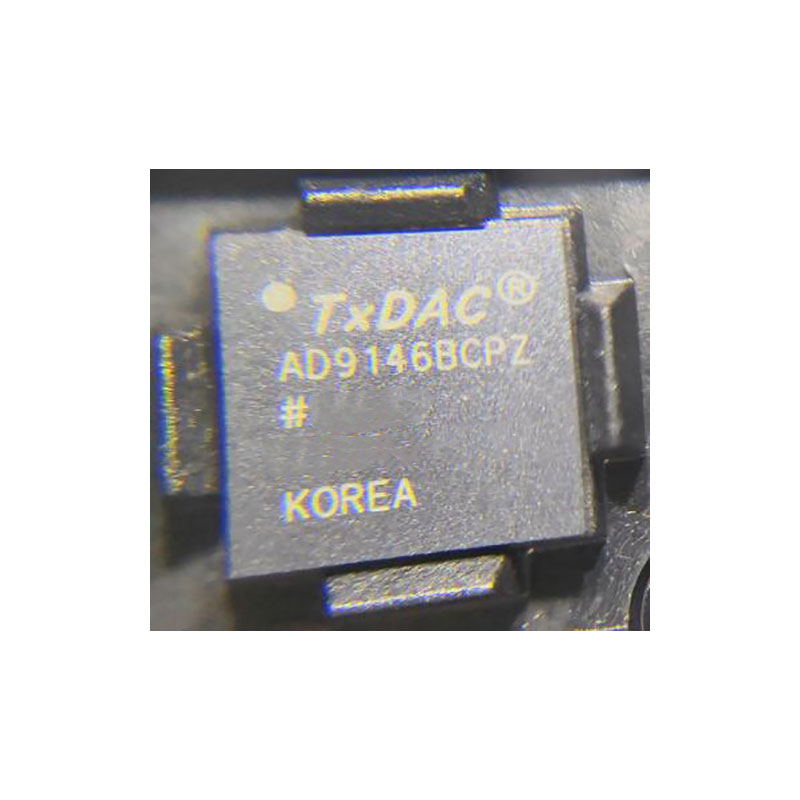
The AD9154BCPZ is a quad, 16-bit, high dynamic range digital-to-analog converter (DAC) that provides a maximum sample rate of 2.4 GSPS, permitting multicarrier generation up to the Nyquist frequency in baseband mode. The AD9154BCPZ includes features optimized for direct conversion transmit applications including complex digital modulation, input signal power detection, and gain, phase, and offset compensation. The DAC outputs are optimized to interface seamlessly with the ADRF6720-27 radio frequency quadrature modulator (AQM) from Analog Devices, Inc. In mix mode, the AD9154BCPZ DAC can reconstruct carriers in the second and third Nyquist Zones. A serial port interface (SPI) provides the programming/readback of internal parameters. The full-scale output current can be programmed over a range of 4 mA to 20 mA.
Caractéristiques:
Supports input data rates up to 1 GSPS
Proprietary, low spurious and distortion design
Single carrier LTE 20 MHz bandwidth (BW), ACLR = 77 dBc at 180 MHz IF
Six carrier GSM IMD = 78 dBc, 600 kHz carrier spacing at 180 MHz IF
SFDR = 72 dBc at 180 MHz IF, −6 dBFS single tone
Flexible 8-lane JESD204B interface
Multiple chip synchronization
Fixed latency
Data generator latency compensation
Input signal power detection
Multiplicateur d'horloge à boucle à verrouillage de phase (PLL) haute performance et à faible bruit
Filtre numérique sincère inverse
Digital quadrature modulation using a numerically controlled oscillator (NCO)
Nyquist band selection—mix mode
Selectable 1×, 2×, 4×, and 8× interpolation filters
Low power: 2.11 W at 1.6 GSPS, full operating conditions
Applications :
Multicarrier LTE and GSM base stations
Wideband repeaters
Software defined radios
Wideband communications
Point to point microwave radio
Transmit diversity, multiple input/multiple output (MIMO)
Automated test equipment
THÉORIE DU FONCTIONNEMENT
The AD9154 is a 16-bit, quad DAC with a SERDES interface.Eight high speed serial lanes carry data into the AD9154.
The clock for the input data is derived from the device clock as called out in the JESD204B specification). This device clock can be sourced with a phase-locked loop (PLL) reference clock used by the on-chip PLL to generate a DAC clock or a high fidelity direct external DAC sampling clock. The device can be configured to operate in one-, two-, four-, or eight-lane modes, depending on the required input data rate. The quad DAC can be configured as a dual link device with each JESD204B link providing data for a dual DAC pair to add application flexibility.
The signal processing datapath of the AD9154 offers four interpolation modes (1×, 2×, 4×, and 8×) through three half-band filters. An inverse sinc filter compensates for DAC output sinc rolloff. A digital inphase and quadrature modulator upcoverts a pair of DAC input signals to an IF frequency within the first Nyquist zone of the DAC programmed into an NCO. Gain, phase, dc offset,and group delay adjustments can programmably predistort the DAC input signals to improve LO feedthrough and unwanted sideband cancellation performance of an analog quadrature modulator following the AD9154 in a transmitter signal chain.
The AD9154 DAC cores provide a differential current output with a nominal full-scale current of 20 mA. The differential current outputs are optimized for integration with the Analog Devices ADRF6720-27 wideband quadrature modulator.
The AD9154 has a mechanism for multichip synchronization,as well as a mechanism for achieving deterministic latency (latency locking). The latency for each DAC remains constant from link establishment to link establishment. The AD9154 makes use of the JESD204B Subclass 1 SYSREF signal to establish multichip synchronization.
The various functional blocks and the data interface must be set up in a specific sequence for proper operation (see the Device
Setup Guide section). This data sheet describes the various blocks of the AD9154 in detail, including descriptions of the JESD204B interface, the control parameters, and the various registers thatset up and monitor the device. The recommended start-up routine reliably sets up the data link.

