Description :
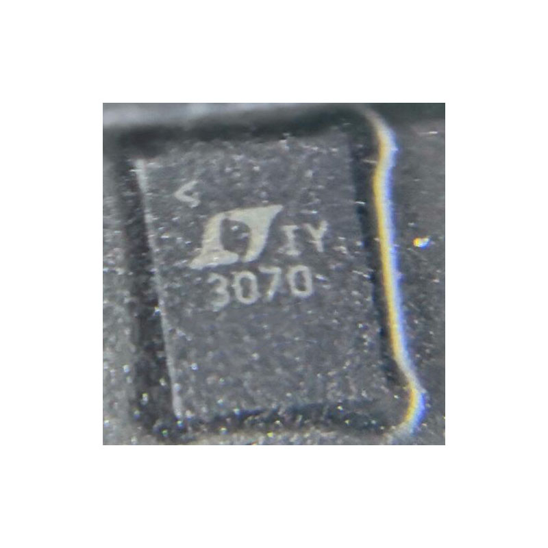
The LT3070IUFD is a low voltage, UltraFast™ transient response linear regulator. The device supplies up to 5A of output current with a typical dropout voltage of 85mV. A 0.01μF reference bypass capacitor decreases output voltage noise to 25μVRMS. The LT3070’s high bandwidth permits the use of low ESR ceramic capacitors, saving bulk capacitance and cost. The LT3070IUFD’s features make it ideal for high performance FPGAs, microprocessors or sensitive communication supply applications.
Output voltage is digitally selectable in 50mV increments over a 0.8V to 1.8V range. A margining function allows the user to adjust system output voltage in increments of ±1%, ±3% or ±5%. The IC incorporates a unique tracking function to control a buck regulator powering the LT3070’s input. This tracking function drives the buck regulator to maintain the LT3070IUFD’s input voltage to VOUT + 300mV, minimizing power dissipation.
Internal protection includes UVLO, reverse-current protection, precision current limiting with power foldback and thermal shutdown.
Caractéristiques:
Output Current: 5A
Dropout Voltage: 85mV Typical
Digitally Programmable VOUT : 0.8V to 1.8V
Digital Output Margining: ±1%, ±3% or ±5%
Low Output Noise: 25μVRMS (10Hz to 100kHz)
Parallel Multiple Devices for 10A or More
Precision Current Limit: ±20%
±1% Accuracy Over Line, Load and Temperature
Stable with Low ESR Ceramic Output Capacitors (15μF Minimum)
High Frequency PSRR: 30dB at 1MHz
Enable Function Turns Output On/Off
VIOC Pin Controls Buck Converter to Maintain Low Power Dissipation and Optimize Efficiency
PWRGD/UVLO/Thermal Shutdown Flag
Current Limit with Foldback Protection
Thermal Shutdown
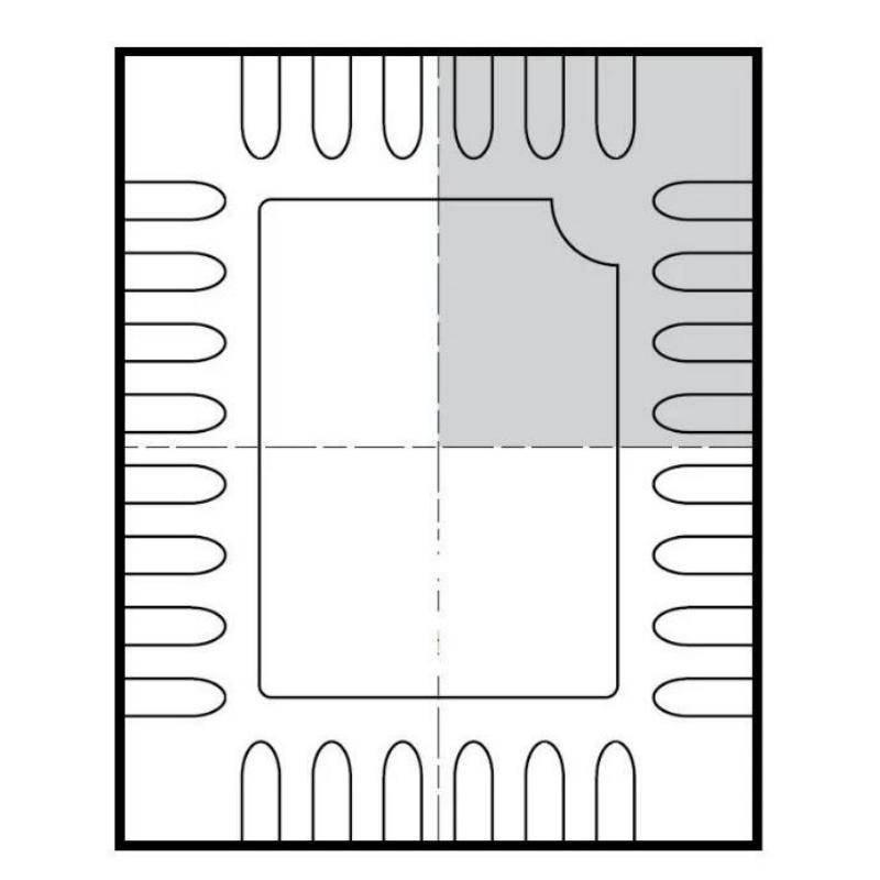
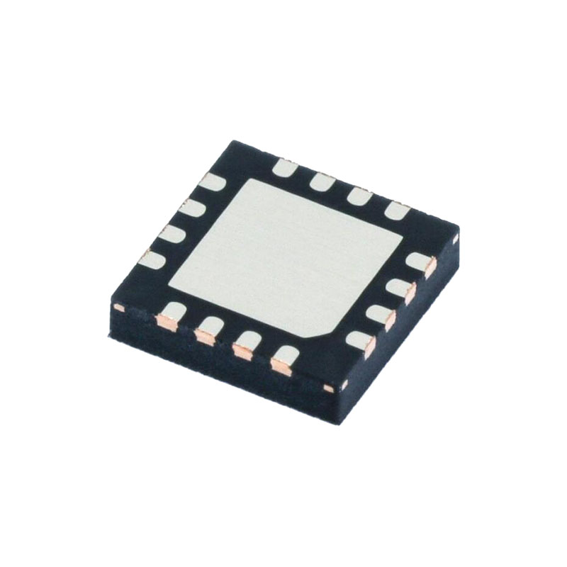
28-Lead (4mm × 5mm × 0.75mm) QFN Package
Applications :
FPGA and DSP Supplies
ASIC and Microprocessor Supplies
Servers and Storage Devices
Post Buck Regulation and Supply Isolation
ABSOLUTE MAXIMUM RATINGS
IN, OUT ………………………………….–0.3V to 3.3V
BIAS ……………………………………. –0.3V to 4V
VO2, VO1, VO0 Inputs ……………… –0.3V to 4V
MARGSEL, MARGTOL Input …………–0.3V to 4V
EN Input ………………………… …….–0.3V to 4V
SENSE Input …………………………. –0.3V to 4V
VIOC, PWRGD Outputs ………………–0.3V to 4V
REF/BYP Output …………………….. –0.3V to 4V
Output Short-Circuit Duration ……..Indefinite
Operating Junction Temperature
LT3070E/LT3070I ………………….. –40°C to 125°C
LT3070MP ……………………………..–55°C to 125°C
Storage Temperature Range ……….–65°C to 150°C
CARACTÉRISTIQUES ÉLECTRIQUES
The denotes the specifications which apply over the full operating temperature range, otherwise specifications are at TA = 25°C. COUT = 15µF (Note 9), VIN = VOUT + 0.3V (Note 5), VBIAS = 2.5V unless otherwise noted.
Note 1: Stresses beyond those listed under Absolute Maximum Ratings may cause permanent damage to the device. Exposure to any Absolute Maximum Rating condition for extended periods may affect device reliability and lifetime.
Note 2: The LT3070 regulators are tested and specified under pulse load conditions such that TJ ≅ TA. The LT3070E is 100% tested at TA = 25°C. Performance at –40°C and 125°C is assured by design, characterization and correlation with statistical process controls. The LT3070I is guaranteed over the –40°C to 125°C operating junction temperature range. The LT3070MP is 100% tested and guaranteed over the –55°C to 125°C operating junction temperature range.
Note 3: To maintain proper performance and regulation, the BIAS supply voltage must be higher than the IN supply voltage. For a given VOUT, the BIAS voltage must satisfy the following conditions: 2.2V ≤ VBIAS ≤ 3.6V and VBIAS ≥ (1.25 • VOUT + 1V). For VOUT ≤ 0.95V, the minimum BIAS voltage is limited to 2.2V.
Note 4: Operating conditions are limited by maximum junction temperature. The regulated output voltage specification does not apply for all possible combinations of input voltage and output current. When operating at maximum output current, limit the input voltage range to VIN < VOUT + 500mV
Note 5: The LT3070 incorporates safe operating area protection circuitry. Current limit decreases as the VIN-VOUT voltage increases. Current limit foldback starts at VIN – VOUT > 500mV. See the Typical Performance Characteristics for a graph of Current Limit vs VIN – VOUT voltage. The current limit foldback feature is independent of the thermal shutdown circuity.
Note 6: Dropout voltage, VDO, is the minimum input to output voltage differential at a specified output current. In dropout, the output voltage equals VIN – VDO.
Note 7: GND pin current is tested with VIN = VOUT(NOMINAL) + 300mV and a current source load. VIOC is a buffered output determined by the value of VOUT as programmed by the VO2-VO0 pins. VIOC’s output is independent of the margining function.
Note 8: Reverse output current is tested with the IN pins grounded and the OUT + SENSE pins forced to the rated output voltage. This is measured as current into the OUT + SENSE pins.
Note 9: Frequency Compensation: The LT3070 must be frequency compensated at its OUT pins with a minimum COUT of 15µF configured as a cluster of (15×) 1µF ceramic capacitors or as a graduated cluster of 10µF/4.7µF/2.2µF ceramic capacitors of the same case size. Linear Technology only recommends X5R or X7R dielectric capacitors.
