Description :
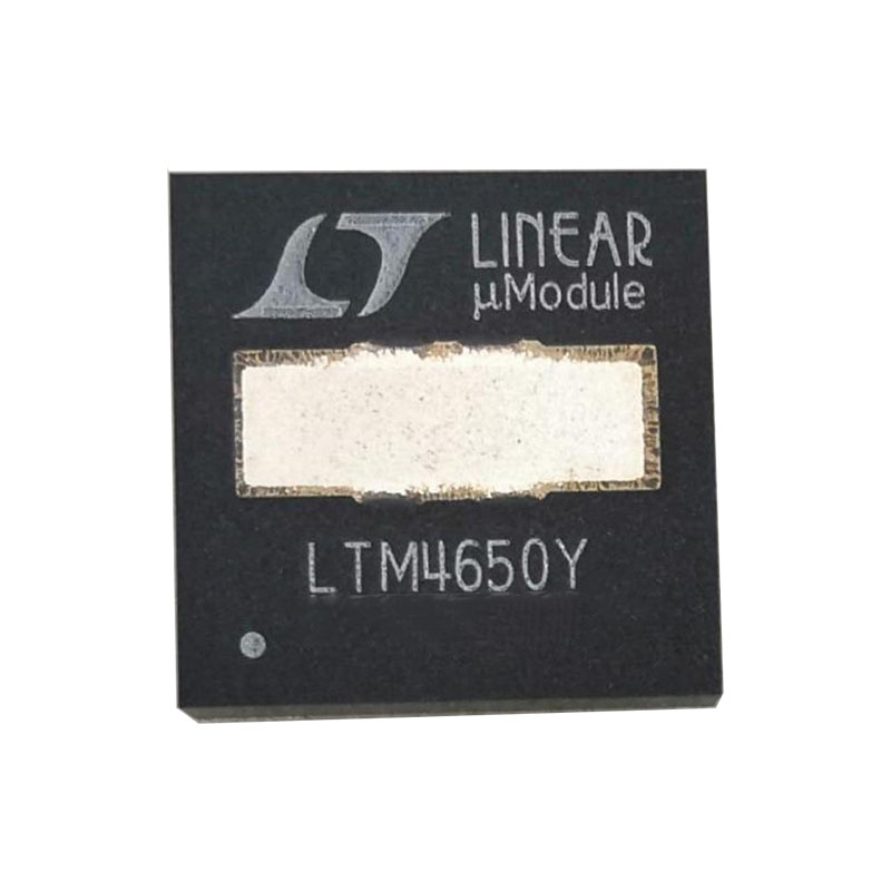
LTM4650 output switch mode buck DC/DC μ Module ® The (power module) voltage regulator is a product with dual channel 25A or single channel 50A. The product comes with a built-in switch controller, power FET, inductor, and all supporting components.
This power module has an output voltage tracking function for power rail sorting, supports multi-phase operation, burst mode operation, and frequency synchronization, and includes a built-in temperature diode responsible for monitoring device temperature.
The input voltage range for LTM4650 operation is 4.5V~15V, and it supports two output voltage ranges of 0.6V~1.8V, which need to be set through a single external resistor. The high-efficiency design of this device can provide a continuous current of 25A for each output. Only a small number of input and output capacitors are needed. The pin compatible model series of LTM4650 includes: LTM4620, LTM4630.
The LTM4650 utilizes high switching frequency and a current mode architecture to achieve fast transient response to voltage and load changes without sacrificing stability.
LTM4650 has overvoltage and overcurrent protection.
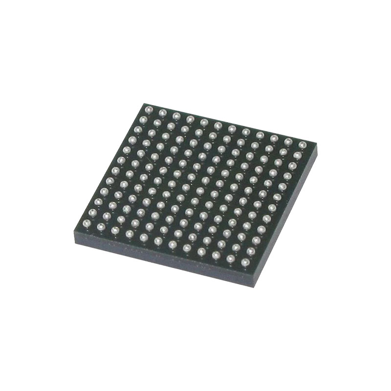
Adopting BGA packaging, the specific dimensions are 16mm * 16mm * 5.01mm.
Caractéristiques:
Dual 25A or Single 50A Output
Input Voltage Range: 4.5V to 15V
Output Voltage Range: 0.6V to 1.8V
±1.5% Maximum Total DC Output Error Over Line, Load and Temperature
Differential Remote Sense Amplifier
Contrôle du mode courant/réponse transitoire rapide
Adjustable Switching Frequency
Synchronisation des fréquences
Overcurrent Foldback Protection
Multiphase Parallel Current Sharing with Multiple LTM4650s Up to 300A
Internal Temperature Monitor
Pin Compatible with the LTM4620 (Dual 13A, Single 26A) and LTM4630 (Dual 18A, Single 36A)
Selectable Burst Mode® Operation
Démarrage progressif/suivi de tension
Output Overvoltage Protection
Applications :
Processor, ASIC and FPGA Core Power
Telecom and Networking Equipment
Storage and ATCA Cards
Industrial Equipment
ORDER INFORMATION
LTM4650EY#PBF SAC305 (RoHS) LTM4650Y e1 BGA 3 –40°C to 125°C
LTM4650IY#PBF SAC305 (RoHS) LTM4650Y e1 BGA 3 –40°C to 125°C
LTM4650IY SnPb (63/37) LTM4650Y e0 BGA 3 –40°C to 125°C
LTM4650MPY#PBF SAC305 (RoHS) LTM4650Y e1 BGA 3 –55°C to 125°C
LTM4650MPY SnPb (63/37) LTM4650Y e0 BGA 3 –55°C to 125°C
Note:Contact the factory for parts specified with wider operating temperature ranges. *Device temperature grade is indicated by a label on the shipping container. Pad or ball finish code is per IPC/JEDEC J-STD-609.
• Recommended LGA and BGA PCB Assembly and Manufacturing Procedures
- LGA and BGA Package and Tray Drawings
Power Derating
The 0.9V and 1.5V power loss curves in Figure 11 and Figure 12 can be used in coordination with the load current derating curves in Figure 13 to Figure 20 for calculating an approximate θJA thermal resistance for the LTM4650 with various heat sinking and airflow conditions. The power loss curves are taken at room temperature, and are increased with a 1.2 multiplicative factor at 120°C. The derating curves are plotted with CH1 and CH2 in parallel single output operation starting at 50A of load with low ambient temperature. The output voltages are 0.9V and 1.5V. These are chosen to include the lower and higher output voltage ranges for correlating the thermal resistance. Thermal models are derived from several temperature measurements in a controlled temperature chamber along with thermal modeling analysis. The junction temperatures are monitored while ambient temperature is increased with and without airflow. The power loss increase with ambient temperature change is factored into the derating curves. The junctions are maintained at ~120°C maximum while lowering output current or power while increasing ambient temperature. The decreased output current will decrease the internal module loss as ambient temperature is increased.

