DESCRIPTION GÉNÉRALE
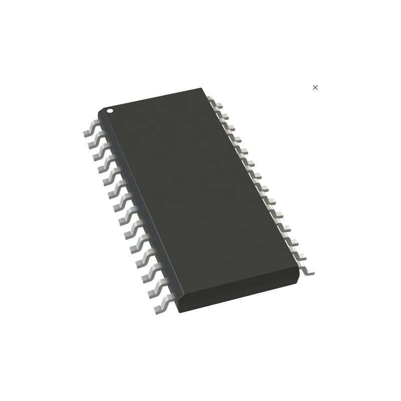
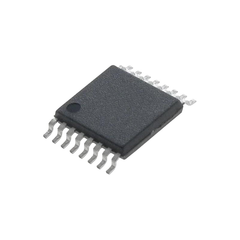
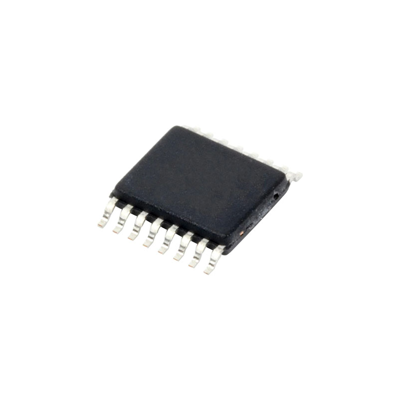
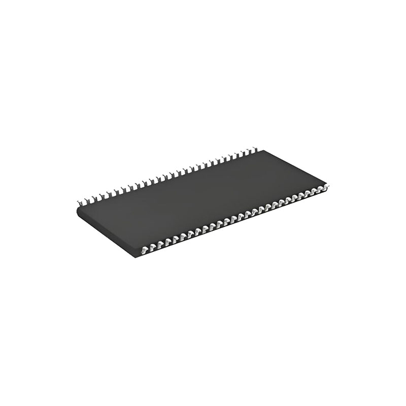
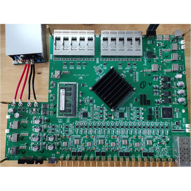
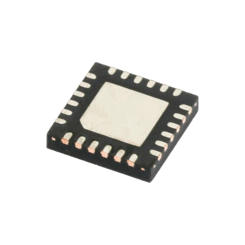
The AD5546 are precision 16-/14-bit, multiplying, low power, current output, parallel input digital-to-analog converters (DACs). They operate from a single 2.7 V to 5.5 V supply with ±10 V multiplying references for four-quadrant outputs. Builtin four-quadrant resistors facilitate the resistance matching and temperature tracking that minimize the number of components needed for multiquadrant applications. The feedback resistor (RFB) simplifies the I-V conversion with an external buffer. The AD5546 are packaged in compact TSSOP-28 packages with operating temperatures from –40°C to +125°C. The EVAL-AD5546SDZ is available for evaluating DAC performance. For more information, see the UG-309 evaluation board user guide.
CARACTÉRISTIQUES
16-bit resolution
14-bit resolution
2- or 4-quadrant multiplying DAC
±1 LSB DNL
±1 LSB INL
Operating supply voltage: 2.7 V to 5.5 V
Low noise: 12 nV/√Hz
Low power: IDD = 10 μA
0.5 μs settling time
Built-in RFB facilitates current-to-voltage conversion
Built-in 4-quadrant resistors allow 0 V to –10 V, 0 V to +10 V, or ±10 V outputs
2 mA full-scale current ±20%, with VREF = 10 V
Automotive operating temperature: –40°C to +125°C
Compact TSSOP-28 package
CANDIDATURES
Équipement d'essai automatique
L'instrumentation
Digitally controlled calibration
Digital waveform generation
CIRCUIT OPERATION
DIGITAL-TO-ANALOG (DAC) CONVERTER SECTION
The AD5546 are 16-/14-bit multiplying, current output, and parallel input DACs. The devices operate from a single 2.7 V to 5.5 V supply and provide both unipolar 0 V to –VREF, or 0 V to +VREF, and bipolar ±VREF output ranges from a –18 V to +18 V reference. In addition to the precision conversion RFB commonly found in current output DACs, there are three additional precision resistors for four-quadrant bipolar applications. The AD5546 consist of two groups of precision R-2R ladders, which make up the 12/10 LSBs, respectively. Furthermore, the four MSBs are decoded into 15 segments of resistor value 2R.Each of the 16 segments in the R-2R ladder carries an equally weighted current of one-sixteenth of full scale. The feedback resistor, RFB, and four-quadrant resistor, ROFS, have values of 10 kΩ. Each four-quadrant resistor, R1 and R2, equals 5 kΩ. In four-quadrant operation, R1, R2, and an external op amp work together to invert the reference voltage and apply it to the REF input. The reference voltage inputs exhibit a constant input resistance of 5 kΩ ±20%. The DAC output, IOUT, impedance is code dependent. External amplifier choice should take into account the variation of the AD5546 output impedance. The feedback resistance in parallel with the DAC ladder resistance dominates output voltage noise. To maintain good analog performance, it is recommended to bypass the power supply with a 0.01 μF to 0.1 μF ceramic or chip capacitor in parallel with a 1 μF tantalum capacitor. Also, to minimize gain error, PCB metal traces between VREF and RFB should match. Every code change of the DAC corresponds to a step function; gain peaking at each output step may occur if the op amp has limited GBP and excessive parasitic capacitance present at the op amp inverting node. A compensation capacitor, therefore, may be needed between the I-V op amp inverting and output nodes to smooth the step transition. Such a compensation capacitor should be found empirically, but a 20 pF capacitor is generally adequate for the compensation. The VDD power is used primarily by the internal logic and to drive the DAC switches. Note that the output precision degrades if the operating voltage falls below the specified voltage. The user should also avoid using switching regulators because device power supply rejection degrades at higher frequencies.
DIGITAL SECTION
The AD5546 have 16-/14-bit parallel inputs. The devices are double buffered with 16-/14-bitregisters. The double-buffered feature allows the update of several AD5546 simultaneously. For the AD5546, the input register is loaded directly from a 16-bit controller bus when the WR pin is brought low. The DAC register is updated with data from the input register when LDAC is brought high. Updating the DAC register updates the DAC output with the new data . To make both registers transparent, tie WR low and LDAC high. The asynchronous RS pin resets the part to zero scale if the MSB pin = 0 and to midscale if the MSB pin = 1.

