DESCRIPTION GÉNÉRALE
The AD5593R has eight input/output (I/O) pins, which can be independently configured as digital-to-analog converter (DAC) outputs, analog-to-digital converter (ADC) inputs, digital outputs, or digital inputs. When an I/O pin is configured as an analog output, it is driven by a 12-bit DAC. The output range of the DAC is 0 V to VREF or 0 V to 2 × VREF. When an I/O pin is configured as an analog input, it is connected to a 12-bit ADC via an analog multiplexer. The input range of the ADC is 0 V to VREF or 0 V to 2 × VREF.
The I/O pins can also be configured to be general-purpose, digital input or output (GPIO) pins. The state of the GPIO pins can be set or read back by accessing the GPIO write data register and GPIO read configuration registers, respectively, via an I2C write or read operation.
The AD5593R has an integrated 2.5 V, 20 ppm/°C reference that is turned off by default and an integrated temperature indicator that gives an indication of the die temperature. The temperature value is read back as part of an ADC read sequence.
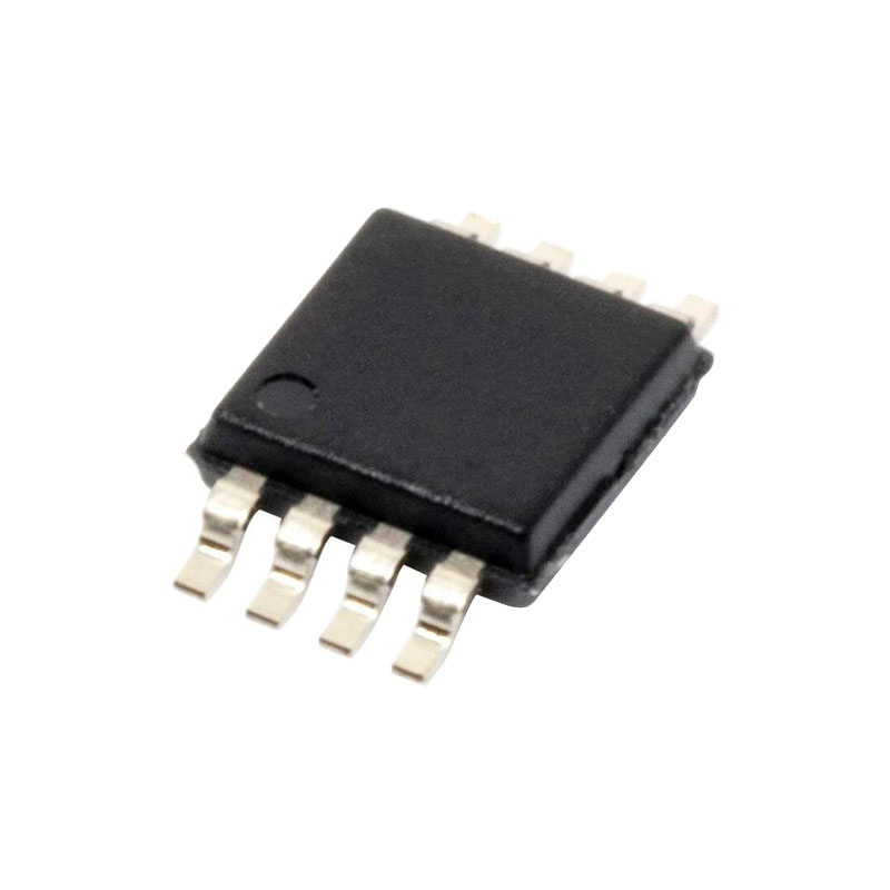
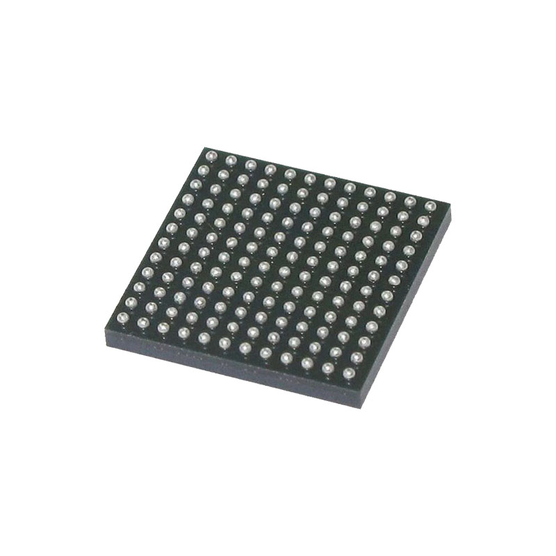
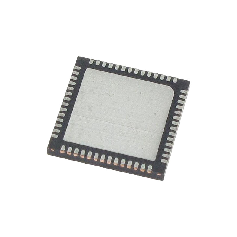
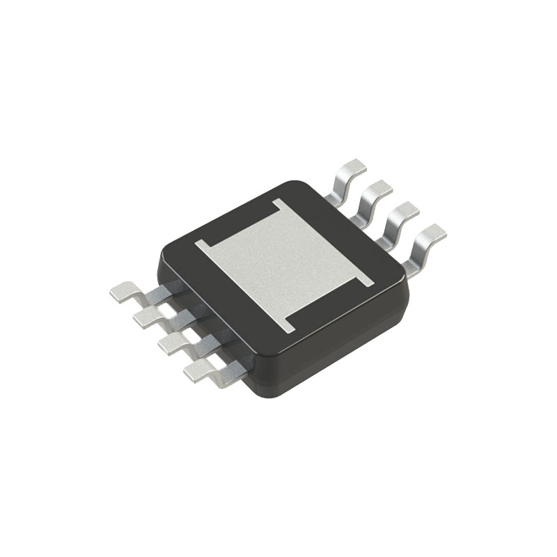
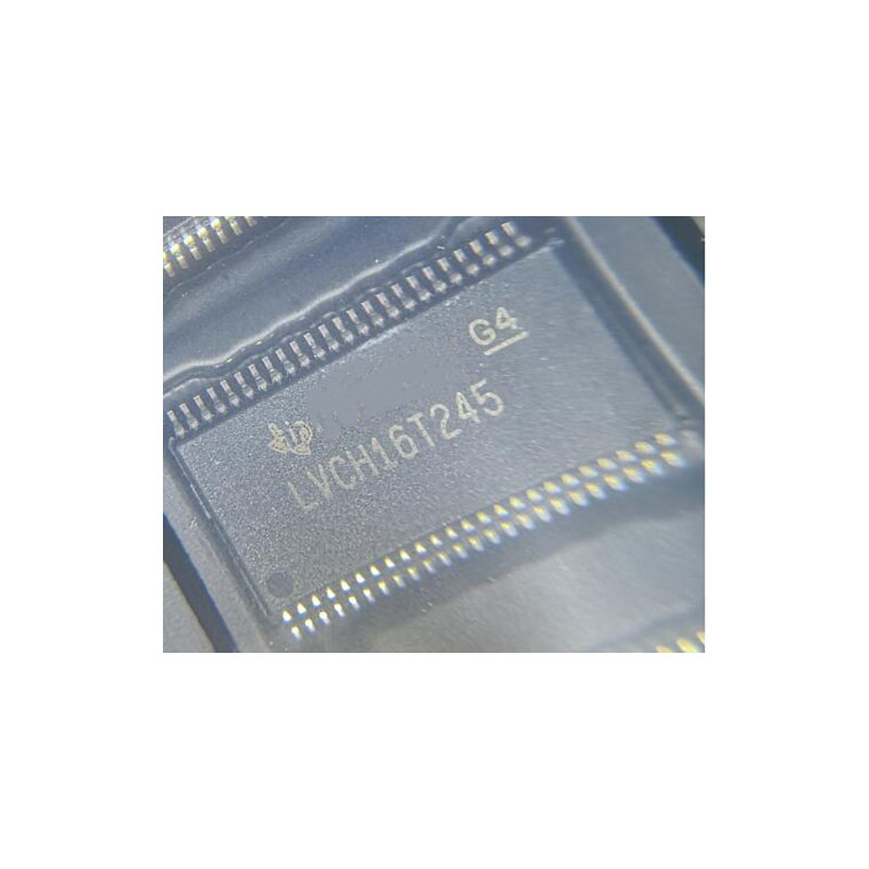
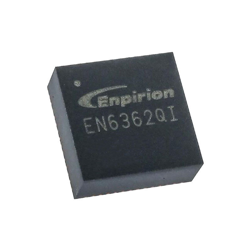
The AD5593R is available in 16-lead TSSOP and LFCSP, as well as a 16-ball WLCSP, and operates over a temperature range of −40°C to +105°C.
CARACTÉRISTIQUES
8-channel, configurable ADC/DAC/GPIO
Configurable as any combination of
8 12-bit DAC channels
8 12-bit ADC channels
8 general-purpose I/O pins
Integrated temperature sensor
16-lead TSSOP and LFCSP and 16-ball WLCSP packages
Interface I²C
CANDIDATURES
Control and monitoring
General-purpose analog and digital I/O
THÉORIE DU FONCTIONNEMENT
The AD5593R is an 8-channel, configurable analog and digital I/O port. The AD5593R has eight pins that can be independently configured as a 12-bit DAC output channel, a 12-bit ADC input channel, a digital input pin, or a digital output pin.
The function of each pin is determined by programming the ADC, DAC, or GPIO configuration registers as appropriate.
DAC SECTION
The AD5593R contains eight 12-bit DACs. Each DAC consists of a
string of resistors followed by an output buffer amplifier.
The DAC channels share a single DAC range bit that sets the output range to 0 V to VREF or 0 V to 2 × VREF. Because the range bit is shared by all channels, it is not possible to set different output ranges on a per channel basis. The input coding to the DAC is straight binary.
Resistor String
The code loaded to the DAC register determines the switch on the string that is connected to the output buffer. Because each resistance in the string has the same value, R, the string DAC is guaranteed monotonic.
DAC Output Buffer
The output buffer is designed as an input/output rail-to-rail buffer. The output buffer can drive 2 nF capacitance with a 1 kΩ resistor in parallel. The slew rate is 1.25 V/μs with a ¼ to ¾ scale settling time of 6 μs. By default, the DAC outputs update directly after data has been written to the input register. The LDAC register delays the updates until additional channels have been written to if required.
DAC Output Range
The DAC output voltage range can be configured to 0 V to VREF (gain = 1) or 0 V to 2 × VREF (gain = 2) using DAC range bit of the general-purpose control register, as shown in Figure 33 and Figure 34, respectively. When VREF = VDD, the 0 V to 2 × VREF range does not allow the DAC to swing the output beyond VDD.
When VREF = VDD for gain = 1 or VREF = 0.5 × VDD for gain = 2, there is an upper dead band of 10 mV at the DAC channel output in unloaded conditions. Additionally, there is a lower dead band of ~4.88 mV at the DAC channel output in unloaded conditions. When drawing a load current at either rail, the output voltage headroom with respect to that rail is limited by the 25 Ω typical channel resistance of the DAC channel. For example, when sinking 1 mA, the minimum output voltage = 25 Ω × 1 mA = 25 mV.


