DESCRIPTION GÉNÉRALE
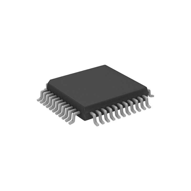
The AD7568 contains eight 12-bit DACs in one monolithic device. The DACs are standard current output with separate VREF, IOUT1, IOUT2 and RFB terminals. The AD7568 is a serial input device. Data is loaded using FSIN, CLKIN and SDIN. One address pin, A0, sets up a device address, and this feature may be used to simplify device loading in a multi-DAC environment. All DACs can be simultaneously updated using the asynchronous LDAC input and they can be cleared by asserting the asynchronous CLR input. The AD7568 is housed in a space-saving 44-pin plastic quad flatpack and 44-lead PLCC.
CARACTÉRISTIQUES
Eight 12-Bit DACs in One Package
4-Quadrant Multiplication
Separate References
Single +5 V Supply
Low Power: 1 mW
Versatile Serial Interface
Simultaneous Update Capability
Reset Function
44-Pin PQFP and PLCC
CANDIDATURES
Process Control
Équipement d'essai automatique
General Purpose Instrumentation
TERMINOLOGY
Relative Accuracy
Relative Accuracy or endpoint linearity is a measure of the maximum deviation from a straight line passing through the endpoints of the DAC transfer function. It is measured after adjusting for zero error and full-scale error and is normally expressed in Least Significant Bits or as a percentage or full-scale reading.
Differential Nonlinearity
Differential nonlinearity is the difference between the measured change and the ideal 1 LSB change between any two adjacent codes. A specified differential nonlinearity of 1 LSB maximum ensures monotonicity.
Gain Error
Gain Error is a measure of the output error between an ideal DAC and the actual device output. It is measured with all 1s in the DAC after offset error has been adjusted out and is expressed in Least Significant Bits. Gain error is adjustable to zero with an external potentiometer.
Output Leakage Current
Output leakage current is current which flows in the DAC ladder switches when these are turned off. For the IOUT1 terminal, it can be measured by loading all 0s to the DAC and measuring the IOUT1 current. Minimum current will flow in the IOUT2 line when the DAC is loaded with all 1s. This is a combination of the switch leakage current and the ladder termination resistor current. The IOUT2 leakage current is typically equal to that in IOUT1.
Output Capacitance
This is the capacitance from the IOUT1 pin to AGND
Output Voltage Settling Time
This is the amount of time it takes for the output to settle to a specified level for a full-scale input change. For the AD7568, it is specified with the AD843 as the output op amp. Digital to Analog Glitch Impulse This is the amount of charge injected into the analog output when the inputs change state. It is normally specified as the area of the glitch in either pA-secs or nV-secs, depending upon whether the glitch is measured as a current or voltage signal. It is measured with the reference input connected to AGND and the digital inputs toggled between all 1s and all 0s.
AC Feedthrough Error
This is the error due to capacitive feedthrough from the DAC reference input to the DAC IOUT terminal, when all 0s are loaded in the DAC.
Channel-to-Channel Isolation
Channel-to-channel isolation refers to the proportion of input signal from one DAC’s reference input which appears at the output of any other DAC in the device and is expressed in dBs.
Digital Crosstalk
The glitch impulse transferred to the output of one converter due to a change in digital input code to the other converter is defined as the Digital Crosstalk and is specified in nV-secs.
Digital Feedthrough
When the device is not selected, high frequency logic activity on the device digital inputs is capacitively coupled through the device to show up as noise on the IOUT pin and subsequently on the op amp output. This noise is digital feedthrough.